REVIEW 4 major objections 6 minor 27 references
Time-resolved study of carbonization and growth of ultrathin 3C-SiC on Si(111) under ultra-high vacuum
T0 review · 4 major / 6 minor · reviewed 2026-08-11 · deepseek-v4-flash
Pith's one-line read Exposing Si(111) to ethylene at 800 °C turns the surface into a 9 nm 3C-SiC layer.
desk verdict A useful time-resolved dataset for C2H4 carbonization of Si(111); the qualitative island-to-coalescence picture is convincing, but the XPS-derived crossover and plateau numbers need an attenuation correction before they are taken literally. read the letter →
The pith
A machine-rendered reading of the paper's core claim, the machinery that carries it, and where it could break.
The reading
What carries the argument
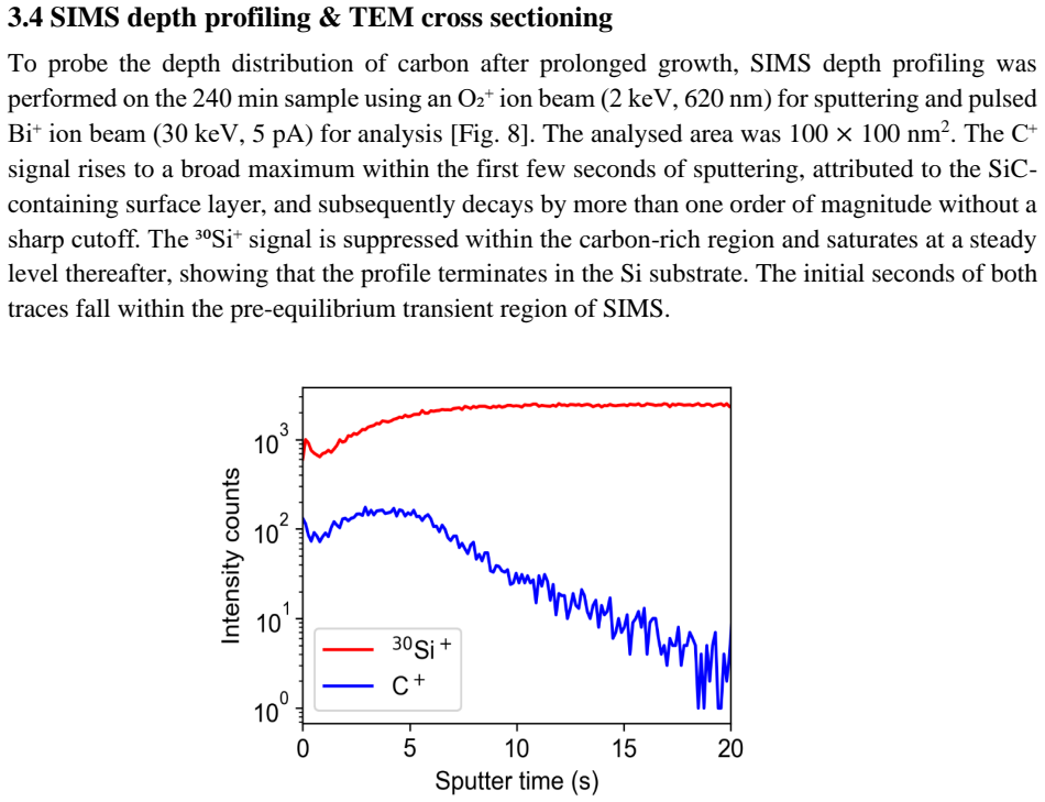
The load-bearing instrument is the time-resolved XPS peak decomposition of the Si 2p doublet: each spectrum is fitted with a fixed 2:1 spin–orbit doublet (0.61 eV splitting, GL(30) line shapes), and the relative areas of the Si–Si and Si–C components are converted directly into elemental-Si and SiC fractions as a function of exposure time. This quantifies the chemical conversion that the morphology story is built on. Supporting the XPS time axis are correlative SEM/AFM height and roughness profiles, site-specific AES C/Si ratios at islands versus valleys, SIMS depth profiling, and STEM/EELS on one FIB-prepared lamella, which together assign the islands to carbide nuclei and the final state to a rough, voided ~9 nm 3C-SiC layer.
What would settle it
Measure the same carbonization with angle-resolved XPS or with a calibrated overlayer-thickness standard: if the elemental-Si signal corrected for inelastic attenuation still leaves about 19–20 percent at saturation, the area-ratio claim survives; if it disappears or the crossover time moves by tens of minutes, the direct conversion of component areas is wrong. Alternatively, cross-section many grains by STEM to see whether 9 nm is the mean thickness or an outlier.
Extended reading notes
Core claim
On clean Si(111) exposed to C2H4 at 800 °C under UHV, silicon converts to cubic silicon carbide through a nucleation–coalescence sequence rather than uniform layer-by-layer growth. The central quantitative evidence is the Si 2p core-level decomposition: the Si–C doublet rises from below 15 percent at 40 min to 81 percent at 220 min and 80.8 percent at 240 min, while the elemental Si doublet falls to about 19 percent and does not vanish. That persistent elemental signal is interpreted as substrate silicon visible through a layer that is not fully continuous, with voids and a rough SiC/Si interface. AES shows carbon enrichment localized at islands; SIMS and STEM/EELS give a layer thickness around 9 nm and identify the zinc-blende 3C-SiC polytype through {111} and {220} interplanar spacings. The paper frames this as a direct time-resolved picture of SiC buffer-layer formation on Si(111), with the reaction saturating rather than proceeding to complete coverage.
Load-bearing premise
The direct conversion of Si 2p component areas into a SiC fraction assumes negligible attenuation of the underlying elemental-Si signal through the growing carbide, and the single 9 nm thickness measured on one island grain in one TEM lamella is taken as representative of the whole layer.
Editorial extensions
If this is right
- After roughly 180–240 min the carbide fraction plateaus near 80–81 percent, so the reaction is self-limiting under these conditions, not complete.
- The residual ~19–20 percent elemental Si signal comes from substrate silicon visible through voids and incomplete coverage, not from a homogeneous partially converted layer.
- SiC nucleates at islands whose carbon content is 2.0–2.3 times that of the surrounding substrate, so early carbonization is spatially localized.
- A near-continuous ~9 nm 3C-SiC layer with sharp local interfaces and a rough average interface is achievable at 800 °C in UHV.
- For buffer applications, the paper suggests that shorter exposures near 80–100 min and lower growth temperatures are preferable to minimize voids.
Reading between the lines
- Beyond the paper: if the elemental-Si XPS signal were corrected for attenuation by the overlying SiC layer, the reported crossover time and 80–81 percent plateau could shift; measuring the same reaction with angle-resolved XPS would test this directly.
- Beyond the paper: the ~9 nm thickness rests on one selected island grain in a single TEM lamella, so the average film thickness could be meaningfully different, which would change the interpretation of the SIMS profile width.
- Beyond the paper: the same island-nucleation framework may apply to other carbide buffer layers grown on Si(111) by reactive carbon exposure, suggesting that void control, not just carbide purity, is the key template-quality parameter.
- Beyond the paper: a practical extension would be to monitor void formation during growth with in-situ scattering or spectroscopic methods, since the paper identifies voids as the main obstacle for subsequent Mo2C growth.
Editorial analysis
A structured set of objections, weighed in public.
Referee Report
Summary. The manuscript reports a time-resolved study of the carbonization of Si(111) by C2H4 exposure at 800 °C under UHV, using in-situ XPS and ex-situ SEM, AFM, AES, SIMS, and STEM/EELS. The authors claim that SiC forms via island nucleation, growth, and coalescence, with the Si 2p carbide component overtaking the elemental component between 120 and 160 min and saturating at 80–81%, leaving about 19–20% elemental Si, and that the resulting layer is a rough, partially continuous 3C-SiC film about 9 nm thick with interfacial voids.
Significance. The qualitative picture—carbidic Si–C appears, islands nucleate and coalesce, and TEM shows a zinc-blende lattice consistent with 3C-SiC—is supported by multiple complementary techniques and is a useful contribution to the sparse literature on Si(111) carbonization. The paper appropriately acknowledges in Section 3.3 that AES does not provide diffraction-based polytype identification and uses TEM as the structural confirmation. The main value is the combined chemical and morphological time sequence. However, the quantitative time course and the 'self-limiting' conclusion currently rest on uncorrected XPS component areas and on a single TEM measurement, so those quantitative claims need revision before they can be considered established.
major comments (4)
- [Section 3.1, Fig. 2(a), Table 2] The Si 2p component areas are converted directly into phase fractions without any attenuation correction for the growing carbide layer. For a patchy overlayer with coverage θ and thickness d, the measured carbide fraction is approximately θ(1−exp(−d/λ)) / [1−θ exp(−d/λ)], where λ is the effective attenuation length; therefore the reported 80–81% plateau and 19–20% residual elemental Si are not equal to the true uncovered surface fraction, and the crossover time between 120 and 160 min is not a direct readout of the converted fraction. Because the interpretation of residual Si as substrate visible through voids (Section 3.1) and the 'self-limiting' conclusion (Section 4) both depend on this ratio, the authors should re-analyze the XPS data with a stratified overlayer model using realistic λ values and the island thickness distribution.
- [Section 3.4, Fig. 10] The reported 9 nm SiC thickness and the 'roughly 50% at composition over the depth from 0 to 9 nm' are extracted from one homogeneous part of one island-grain in a single FIB lamella. No statistics over multiple grains or lamellae and no uncertainty estimate are provided. Since the XPS interpretation in Section 3.1 relies on the thickness of the carbide layer, the representativeness of this single 9 nm value must be demonstrated.
- [Section 3.1, Table 2, Fig. 2(a)] No error bars, replicate measurements, or fitting-sensitivity analysis are reported. Each time point corresponds to a single sample and a single CasaXPS fit with fixed FWHM, GL(30) line shape, and 2:1 doublet ratio; the quoted fractions (85.2%, 73.7%, 81.1%, 80.8%) are presented without any uncertainty. The quantitative curve in Fig. 2(a) should include uncertainties and a demonstration that the crossover time and saturation plateau are robust to reasonable variation of the fitting constraints.
- [Section 3.4, Fig. 10(c)] The interplanar spacings of 2.60 Å and 1.62 Å are assigned to {111} and {220} planes of 3C-SiC, but the corresponding bulk 3C-SiC values are approximately 2.52 Å and 1.54 Å. The 3–5% discrepancy requires an explanation (e.g., strain, calibration, or measurement uncertainty). Without this, the d-spacing evidence for the 3C polytype is weaker than stated, although the growth conditions and the observed symmetry are supportive.
minor comments (6)
- [Table 2 and Section 3.1] Table 2 lists a growth time of '220 min' and a saturation value at that time, while the growth-duration list, Fig. 1, and the text use 240 min; please clarify which exposure time is correct.
- [Section 3.1, Fig. 2] The y-axis label 'relative fractions of phases in the modified layer' should be defined more precisely; the reader needs to know whether these are signal-area ratios or atomic fractions, especially because the two are not identical without matrix and attenuation corrections.
- [Section 3.1] The statement that the high C–Si fraction (>90%) from C 1s and the saturating Si–C fraction (~81%) from Si 2p provide 'internally consistent evidence' is not directly justified, because C 1s and Si 2p probe different depths and have different sensitivity factors; this should be reworded or quantified.
- [Section 3.2] There are several typographical issues, including 'In [Fig. 3(a)] these terraces are obviously seen by the decoration of the SiC islands' (brackets and wording), 'SEM images of of SiC nanostructures,' and 'the two the longest exposures'; these should be corrected.
- [Section 3.4] Reference [26] appears to contain duplicated author text ('J.P. Li, A.J. Steckl, J. J.P. Li, A.J. Steckl, J.'); please fix the reference formatting.
- [Conclusion] The term 'Mo2C MXenes' is used without introduction; consider clarifying the connection to the earlier discussion of 2D Mo2C growth and provide the appropriate context or reference.
Circularity Check
No circularity found: the central claims are direct experimental measurements checked against published reference values, with no fitted-input-as-prediction or load-bearing self-citation.
full rationale
The paper's principal claims—the progressive rise of the SiC component in Si 2p spectra to 80–81%, the accompanying morphological progression from islands to a coalesced layer, the localized carbon enrichment at AES island sites, and the identification of 3C-SiC by TEM interplanar spacings—are all direct measurements, not outputs of a fitted model that presupposes the result. The SiC fraction is defined operationally as the fitted Si 2p Si–C component area normalized within the Si 2p doublet, and the paper explicitly states that the plotted fractions are those areas (Table 2, Section 3.1), so no hidden reduction occurs. The binding-energy assignments are checked against published literature ranges rather than derived from the claim. The polytype assignment is initially inferred from growth conditions with external citations and then independently confirmed by STEM/EELS lattice-spacing measurements against known 3C-SiC and Si values, so the confirmation is not circular. The only self-citation is reference [14], which describes the UHV apparatus and is not load-bearing for any scientific conclusion. The skeptical concern about attenuation of the elemental-Si signal through the growing carbide layer is a legitimate quantitative refinement of the reported fractions, but it does not make the derivation circular: the paper's fraction is what it says it is, a signal-ratio measurement, and the paper's own interpretation of the residual silicon signal is separately supported by AFM and TEM observations. No step reduces by construction to its own inputs, and no load-bearing claim rests on an unverified self-citation.
Assumptions & free parameters
free parameters (1)
- XPS Si 2p peak-fitting constraints =
FWHM 0.61 eV, spin-orbit splitting 0.61 eV, doublet intensity ratio 2:1
assumptions (6)
- domain assumption XPS chemical-state assignments follow published binding energies for elemental Si and SiC.
- domain assumption Fixed XPS lineshape constraints are valid for all Si 2p fits.
- domain assumption Si 2p component area ratios map linearly to phase fractions without attenuation correction.
- domain assumption Separate samples prepared for each exposure time form a single time course.
- domain assumption At 800 C and 2.5e-4 Pa, ethylene dissociates completely, and hydrogen desorption leaves carbon as the only reacting species.
- domain assumption The SIMS erosion rate remains constant across the SiC layer and the Si substrate.
Cite this review
Pith. "Pith review of Time-resolved study of carbonization and growth of ultrathin 3C-SiC on Si(111) under ultra-high vacuum." pith.science (2026). https://pith.science/paper/MGCV57EM
@misc{pith2026260809431,
  author       = {Pith},
  title        = {Pith review of: Time-resolved study of carbonization and growth of ultrathin 3C-SiC on Si(111) under ultra-high vacuum},
  year         = {2026},
  howpublished = {\url{https://pith.science/paper/MGCV57EM}},
  note         = {Machine review of arXiv:2608.09431}
}
abstract
The early-stage formation of silicon carbide (SiC) on Si(111) by ethylene exposure under ultra-high vacuum (UHV) was investigated to resolve the time-dependent chemical and morphological evolution of an ultrathin layer. Clean Si(111) substrates were exposed to C$_2$H$_4$ at 800 {\deg}C for 2 min to 4 h, and the surfaces followed by in-situ X-ray photoelectron spectroscopy (XPS) and ex-situ AFM, SEM, AES, SIMS and TEM. Si 2p and C 1s peak analysis shows the progressive conversion of elemental silicon into a carbidic Si-C phase, the SiC fraction overtaking the elemental component between 120 and 160 min and saturating near 80-81% beyond 180 min, leaving about 19-20% residual elemental silicon. Correlative SEM and AFM reveal a parallel morphological progression, from sparse isolated islands to a coalesced, near-continuous layer. AES depth profiling confirms carbon incorporated into the near-surface region rather than weakly adsorbed as contamination, assigning the islands to early SiC nuclei. TEM confirms the zinc-blende lattice and the presence of cubic silicon carbide (3C-SiC). Together, these results provide a time-resolved picture of SiC nucleation, coalescence and layer growth on Si(111), relevant to 3C-SiC heteroepitaxy, and can be utilized in the optimization of SiC/Si(111) templates for growth of III-nitride and other carbide systems on silicon (e.g. Mo$_2$C).
Figures


Figures from the paper (3 more)


Reference graph
Works this paper leans on
-
[1]
A. Severino, C. Locke, R. Anzalone, M. Camarda, N. Piluso , A. La Magna, S.E. Saddow, G. Abbondanza, G. D’Arrigo, F. La Via, 3C -SiC film growth on Si substrates, ECS Trans. 35 (6) (2011) 99
work page 2011
-
[2]
B. Wang, J. Yin, D. Chen, X. Long, L. Li, H. -H. Lin, D.N. Talwar, R. -X. Jia, Y. -M. Zhang, I.T. Ferguson, W. Sun, Z.C. Feng, L. Wan, Optical and surface properties of 3C -SiC thin epitaxial films grown at different temperatures on 4H-SiC substrate, Superlattices Microstruct. 156 (2021) 106960
work page 2021
-
[3]
F. Li, F. Roccaforte, G. Greco, P. Fiorenza, F. La Via, A. Pérez -Tomas, J.E. Evans, C.A. Fisher, F.A. Monaghan, P.A. Mawby, M. Jennings, Status and prospects of cubic silicon carbide power electronics device technology, Materials 14 (19) (2021) 5831
work page 2021
-
[4]
J.B. Casady, R.W. Johnson, Status of silicon carbide (SiC) as a wide-bandgap semiconductor for high- temperature applications: a review, Solid-State Electron. 39 (10) (1996) 1409–1422
work page 1996
-
[5]
S. Nishino, J.A. Powell, H.A. Will, Production of large -area single-crystal wafers of cubic SiC for semiconductor devices, Appl. Phys. Lett. 42 (5) (1983) 460–462. 16
work page 1983
- [6]
-
[7]
L.-O. Björketun, L. Hultman, I.P. Ivanov, Q. Wahab, J.-E. Sundgren, Interfacial void formation during vapor phase growth of 3C -SiC on Si(001) and Si(111) substrates – characterization by transmission electron microscopy, J. Cryst. Growth 182 (1997) 379–388
work page 1997
-
[8]
Y. Watanabe, T. Horikawa, K. Kamimura, The influence of the carbonization mechanisms on the crystalline quality of the carbonization layer for heteroepitaxial growth of 3C -SiC, Mater. Sci. Forum 778–780 (2014) 230–233. [9 ] K. Tonisch, W. Jatal, F. Niebelschütz, H. Romanus, U. Baumann, F. Schwierz, J. Pezoldt, AlGaN/GaN- heterostructures on (111) 3C -SiC...
work page 2014
Show all 27 references
-
[10]
M.S. Hu, L.S. Hong, Surface carbonization of Si(111) by C2H2 and the subsequent SiC(111) epitaxial growth from SiH4 and C2H2, J. Cryst. Growth 265 (2004) 382
2004
-
[11]
Perova, J
T.S. Perova, J. Wasyluk, S.A. Kukushkin, A.V. Osipov, N.A. Feoktistov, S.A. Grudinkin, Micro - Raman mapping of 3C-SiC thin films grown by solid–gas phase epitaxy on Si(111), Nanoscale Res. Lett. 5 (2010) 1507
2010
-
[12]
Milenov, I
T. Milenov, I. Avramova, V. Mehandziev, I. Zahariev, G. Avdeev, D. Karashanova, B. Georgieva, B. Blagoev, K. Kirilov, P. Rafailov, S. Kolev, D. Dimov, D. Karaivanova, D. Kalchevski, D. Trifonov, I. Grozev, V. Popov, A comparative study on synthesizing SiC via carbonization of ...
2025
-
[13]
C. Xu, L. Wang, Z. Liu, L. Chen, J. Guo, N. Kang, X.-L. Ma, H.-M. Cheng, W. Ren, Large-area high- quality 2D ultrathin Mo 2C superconducting crystals, Nat. Mater. 14 (2015) 1135 –1141. https://doi.org/10.1038/nmat4374
2015 doi
-
[14]
Voborný, M
S. Voborný, M. Kolíbal, J. Mach, J. Čechal, P. Bábor, S. Průša, J. Spousta, T. Šikola, Deposition and in-situ characterization of ultra-thin films, Thin Solid Films 459 (2004) 17–22
2004
-
[15]
Takagaki, Y
T. Takagaki, Y. Igari, T. Takaoka, I. Kusunoki, XPS study of the reaction of the Si(100) surface with a C2H4 beam, Appl. Surf. Sci. 92 (1996) 287
1996
-
[16]
Himpsel, F.R
F.J. Himpsel, F.R. McFeely, A. Taleb-Ibrahimi, J.A. Yarmoff, G. Hollinger, Microscopic structure of the SiO2/Si interface, Phys. Rev. B 38 (1988) 6084
1988
-
[17]
Severino, G
A. Severino, G. D’Arrigo, C. Bongiorno, S. Scalese, F. La Via, G. Foti, Thin crystalline 3C-SiC layer growth through carbonization of differently oriented Si substrates, J. Appl. Phys. 102 (2007) 023518
2007
-
[18]
Kusunoki, Y
I. Kusunoki, Y. Igari, XPS study of a SiC film produced on Si(100) by reaction with a C 2H2 beam, Appl. Surf. Sci. 59 (1992) 95–104
1992
-
[19]
Delplancke, J.M
M.P. Delplancke, J.M. Powers, G.J. Vandentop, M. Salmeron, G.A. Somorjai, Preparation and characterization of amorphous SiC:H thin films, J. Vac. Sci. Technol. A 9 (3) (1991) 450–455
1991
-
[20]
Önneby, C.G
C. Önneby, C.G. Pantano, Silicon oxycarbide formation on SiC surfaces and at the SiC/SiO2 interface, J. Vac. Sci. Technol. A 15 (1997) 1597–1602
1997
-
[21]
Fujita, Y
K. Fujita, Y. Kusumi, M. Ichikawa, Nucleation along step edges during Si epitaxial growth on the Si(111) surface observed by STM, Surf. Sci. 380 (1997) 66–74. 17
1997
-
[22]
Ishikawa, N
Y. Ishikawa, N. Ikeda, M. Kenmochi, T. Ichinokawa, UHV-SEM observations of cleaning process and step formation on silicon (111) surfaces by annealing, Surf. Sci. 159 (1985) 256–264
1985
-
[23]
Borowik, N
Ł. Borowik, N. Chevalier, D. Mariolle, E. Martinez, F. Bertin, A. Chabli, J.C. Barbé, Controlled synthesis of SiC nanoparticles from surface silicon contamination, Thin Solid Films 527 (2013) 133– 136
2013
-
[24]
G. Ecke, H. Rößler, V. Cimalla, J. Pezoldt, T. Stauden, Auger investigations of thin SiC films, Fresenius J. Anal. Chem. 361 (1998) 564–568
1998
-
[25]
Mogab, H.J
C.J. Mogab, H.J. Leamy, Conversion of Si to epitaxial SiC by reaction with C₂H₂, J. Appl. Phys. 45 (1974) 1075
1974
-
[26]
J.P. Li, A.J. Steckl, J. J.P. Li, A.J. Steckl, J. Microstructural investigation of low temperature chemical vapor deposited 3C -SiC/Si thin films using single -source precursors, Electrochem. Soc. 142 (1995) 634
1995
-
[27]
Scholz, U
R. Scholz, U. Gösele, F. Wischmeyer, E. Niemann, Prevention of micropipes and voids at β - SiC/Si(100) interfaces, Appl. Phys. A 66 (1998) 59
1998
-
[28]
L. Wang, G. Walker, J. Chai, A. Iacopi, A. Fernandes, S. Dimitrijev , Kinetic surface roughening and wafer bow control in heteroepitaxial growth of 3C-SiC on Si(111) substrates, Sci. Rep. 5 (2015) 15423
2015
Reviewed August 11, 2026 · model on record in the stance chip above.
Discussion (0). Continue with ORCID to comment.