REVIEW 3 major objections 5 minor 71 references
The paper identifies a previously unrecognized decoherence mechanism in superconducting circuits: microwave-driven Coulomb blockade in metallic grains, which is as common and as damaging as two-level-system defects.
Reviewed by Pith at T0; open to challenge. T0 means a machine referee read the full paper against a public rubric. the ladder, T0–T4 →
T0 review · deepseek-v4-flash
2026-08-01 23:43 UTC pith:OYDVHODV
load-bearing objection Strong experimental evidence for a new, natural decoherence mechanism in superconducting circuits, with one overconfident fit that violates the model's stated regime; worth refereeing carefully. the 3 major comments →
Coulomb blockade in microscopic material defects as a source of decoherence and noise in solid-state quantum circuits
The pith
A machine-rendered reading of the paper's core claim, the machinery that carries it, and where it could break.
Core claim
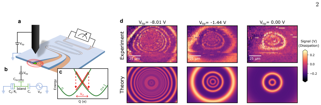
In a superconducting resonator, a small metallic island (grain) tunnel-coupled to a reservoir and capacitively coupled to the resonator's microwave field forms a defect. Near a charge degeneracy point, the microwave voltage alternately favors charge states n and n+1; each cycle an electron tunnels on and off, dissipating energy (Sisyphus dissipation) and stochastically shifting the offset charge, producing both loss and noise. The authors show the observed concentric-ring patterns in scanning gate images, equally spaced voltage peaks, power independence, and simultaneous loss/frequency data are all captured by an Anderson–Holstein-type impurity with Orthodox single-electron tunneling rates.
What carries the argument
The central object is the 'Sisyphus defect': a metallic island with discrete charge states, tunnel-coupled to an electronic reservoir and capacitively coupled to a resonator's microwave voltage. The key identity is the linear-response prediction that a drive-induced charge fluctuation produces a resonator frequency shift δω = -AΓ²/(2(Γ²+ω0²)) and dissipation δκ = Aω0Γ/(Γ²+ω0²), so that at the degeneracy point δω/δκ = -Γ/2ω0 with Γ proportional to the tunnelling rate. This identity connects the measured loss and dispersive shift to the defect's tunnel resistance and charging energy, allowing fits that identify the defects as metallic grains.
Load-bearing premise
The model's quantitative fits and identification of the defects as metallic grains rely on the Orthodox-theory/linear-response treatment remaining valid for a fitted tunnel resistance of 15 kΩ, which is below the quantum resistance ≈25.8 kΩ where the weak-coupling condition (Rt >> h/e²) fails.
What would settle it
Measure the loss and frequency-shift peaks of a defect whose tunnel resistance is tuned across RK (e.g., by changing oxide thickness or gate voltage) and check whether the peak width, temperature dependence, and the ratio δω/δκ follow the analytic expressions; if they deviate below RK as predicted by strong-coupling renormalization, the quantitative identification breaks down. Alternatively, a device fabricated on an epitaxial film with no grain boundaries should show no Sisyphus rings.
If this is right
- Loss from these defects is power-independent, so standard saturation-based TLS characterization will misattribute it to other power-independent processes.
- The mechanism persists as temperature approaches zero, so simply cooling a device does not suppress it.
- Because the defects are as common as TLS defects, they can by themselves limit coherence to millisecond timescales with only a handful of defects.
- Removing metallic grains during fabrication, for example by epitaxial film growth, is a direct mitigation strategy.
- Since the loss scales with the zero-point microwave field amplitude near resonator edges, devices with stronger edge fields will be more affected.
Where Pith is reading between the lines
- If Sisyphus defects are as prevalent as suggested, published TLS densities may be systematically overestimated, since Sisyphus loss is power-independent and could be counted as TLS in saturation measurements; reanalyzing existing power-series data could separate the two.
- The δω/δκ ratio offers a quick diagnostic: a device-level measurement of the ratio at a charge degeneracy directly gives the defect tunnel resistance, so one could screen fabrication processes without a scanning gate microscope.
- The model predicts a specific scaling of peak loss with device frequency (Rt ∝ 1/fres for maximal dissipation); testing this across a family of resonator frequencies would provide a falsifiable check.
- The reported abundance implies that single-grain statistical models (grain size distribution, oxide-barrier transparency) could predict coherence yields for a given thin-film process.
Editorial analysis
A structured set of objections, weighed in public.
Referee Report
Summary. The paper reports scanning gate microscopy (SGM) measurements on live superconducting resonators and attributes a set of loss features to a previously unrecognised decoherence mechanism: microwave-driven single-electron tunnelling in unintentional metallic grains ('Sisyphus defects'). The experimental signatures are compelling and mutually consistent: concentric rings in S21(x,y) that shrink with tip voltage; more than twenty equidistant periodic peaks in Vtip; stochastic offset-charge jumps; a response independent of microwave power, in contrast to the saturable TLS signature visible in the same dataset; and β≈1 scaling of the voltage periodicity with tip–defect distance. The authors fit the measured loss κ(Vtip) and frequency shift δf(Vtip) with a linear-response model derived from an Anderson–Holstein Hamiltonian and Orthodox-theory tunnelling rates (SI §IV), extracting Rt = 600 kΩ, Cj = 0.1 fF (Fig. 2d) and Rt = 15 kΩ, Cj = 0.35 fF (Fig. 2f). Ex-situ XRR, GIXRD, SEM and AFM data indicate 10–30 nm grains in the Nb films, and a COMSOL model of the tip–island capacitance independently suggests a ~12 nm grain. Fourier-spectrogram analysis identifies four spatially distinct defects in one scan frame, and similar defects are found on all three resonators studied.
Significance. If the identification holds, the paper makes an important contribution: it links a class of power-independent microwave loss in superconducting circuits to a concrete microscopic object (a Coulomb-blockaded metallic grain) with a clear fabrication-mitigation route, and it shows that a subset of loss normally attributed to TLS would be systematically misattributed. The strengths are real: the qualitative signatures are largely parameter-free and mutually corroborating; the linear-response derivation in SI §IV is transparent; the ratio δω/δκ = −Γ/2ω0 at degeneracy provides a parameter-free consistency check on Rt; the Fourier decomposition (SI §VIII) is a careful and convincing way to disentangle overlapping defects; and the ex-situ characterisation corroborates the grain hypothesis. The main risk is quantitative, not qualitative: the paper's most consequential numbers — the ~5 kHz loss, the Fig. 3 parameter-space placement, and the 'as debilitating as TLS' claim — rest on fits performed at parameters where the manuscript itself states the Orthodox model is no longer strictly valid.
major comments (3)
- [Main text Discussion; SI §IV; Figs. 2f, 3] The stress-test concern lands and is grounded in the manuscript's own text. SI §IV defines the Orthodox regime by the weak-coupling condition Rt >> RK, and the fits use the linear-response expressions (S32–S37) derived under that assumption via rate equation (S14). The Discussion concedes that for Rt ≲ h/e2 'the Orthodox treatment is no longer strictly valid', yet Fig. 2f is fitted with these expressions to Rt = 15 kΩ < RK ≈ 25.8 kΩ, and that fit anchors the Fig. 3 parameter placement and the ~5 kHz loss estimate. Moreover, Fig. 3's dissipation maximum at f = 6.7 GHz, T ≈ 200 mK occurs at Rt ≈ 16 kΩ (Γ = ω0), i.e. the highest-impact regime is precisely the regime where the model is admittedly invalid. Please quantify cotunneling/phase-fluctuation corrections at G ≈ GQ (e.g. P(E) or diagrammatic treatment), or restrict quantitative parameter extraction to the weak-coupling defect and pres
- [Main text, Abundance and Discussion] The headline claim that Sisyphus defects are 'as common and as debilitating to device performance as TLS defects' is extrapolated from three resonators on two samples, small scan regions, and a detection method the authors themselves describe as Nyquist-limited and coupling-threshold-limited. No estimate is given of detection bias, defect density (linear or areal), or the fraction of defects missed; the 10% duty-cycle argument supports impact per defect but not abundance. A lower-bound density estimate per unit edge length/area, stated together with the detection threshold, would quantify the claim; otherwise the comparison to TLS incidence should be tempered.
- [SI §V.A; Fig. 2d; Fig. S8] For the weak-coupling defect (Rt = 600 kΩ, Cj = 0.1 fF, T ≈ 100 mK), the model's thermal FWHM (δng,FWHM ≈ 0.04) is reported as ~3× narrower than the observed peak, and no T-dependence of the width is seen up to 1.1 K (Fig. S8). The Fig. 2d fit therefore achieves its line shape only through an uncharacterised broadening source (environmental charge noise) that is not in the stated parameter set. Since the same fit constrains Cj/Ec and feeds the quantitative loss estimate, please report the effective broadening used in the fit and its sensitivity, or state the implied uncertainty on Cj.
minor comments (5)
- [SI §V.A] Numerical check: with Cj = 0.1 fF (CΣ ≈ 0.1 fF) and T = 100 mK, Eq. (S41) gives δng,FWHM ≈ 0.02, not the quoted 0.04; the quoted value corresponds to T ≈ 200 mK. The same factor-of-two discrepancy appears in the Cj = 0.35 fF example (quoted 0.25 vs ~0.13 at 200 mK). Please verify, as it affects the comparison with the observed widths.
- [Main text Discussion (1e vs 2e)] The use of 1e periodicity in a superconducting system is asserted with a brief justification via Nb-specific behaviour and the lack of temperature dependence (ref. 53). A sentence quantifying the expected size of 2e/Cooper-pair corrections to the rates would strengthen this assumption.
- [Fig. 1d caption] The statement that 'the only parameter varied between the simulation frames is the tip voltage' should be clarified: the underlying simulation parameters were fitted to the same defect (Fig. 2d), so the ring-pattern reproduction is a consistency check rather than a parameter-free prediction.
- [SI §III.B vs §V] The power-independence range is quoted as 'up to ⟨N⟩ ~ 10^4' in SI §III.B but 'up to ~10^6' in SI §V. Please state the experimental range consistently in both places.
- [SI §III.A vs main text] The main text reports 'over 20 equidistant peaks on either side of Vtip = 0', while SI §III.A reports 'more than 20 peaks' in total. Please make the count consistent.
Circularity Check
No significant circularity: the model fits are transparent and independently cross-checked.
full rationale
The paper is a fitting-and-characterisation study rather than a parameter-free prediction exercise, and it does not disguise its fits as predictions. The Anderson–Holstein/Orthodox model (Eqs. S1–S37) is presented as an external theoretical framework (Averin–Likharev, Persson et al.), not as a self-citation or an ansatz imported solely from the authors' prior work. The load-bearing identification of the defects as Coulomb-blockaded metallic grains rests on observed signatures that are not fed into the fit: equidistant voltage peaks, stochastic offset-charge jumps, power independence of the response, the parameter-free ratio δω/δκ = −Γ/2ω0 = −(RK/Rt)(kBT/ℏω0) at charge degeneracy, and ex-situ XRR/GIXRD/SEM grain-size estimates (~21 nm) that independently cross-check the electrostatic COMSOL estimate (rg ≈ 12 nm) and the fitted Cj ≈ 0.1 fF. The Fourier/spectrogram defect identification assumes a β = 1 distance scaling and then verifies β ≈ 1, which is an honest consistency test rather than a circular reduction. The self-citations (Hegedüs et al. for the SGM setup, de Graaf et al. for related SGM studies) concern instrumentation and analysis methods and are not used to justify the central physical mechanism. The acknowledged breakdown of the Orthodox treatment for Rt ≲ h/e² — relevant to the Fig. 2f defect with fitted Rt = 15 kΩ — is a model-validity and uncertainty concern, not a circularity: the model inputs are not defined in terms of the conclusions, and the quantitative identification is cross-checked by independent material characterisation. No step reduces, by construction, to its own inputs.
Axiom & Free-Parameter Ledger
free parameters (10)
- Rt (defect in Fig. 2d) =
600 kΩ
- Cj (defect in Fig. 2d) =
0.1 fF
- Cr (defect in Fig. 2d) =
5e-6 fF
- Ctip (defect in Fig. 2d) =
3.25e-5 fF
- Rt (defect in Fig. 2f) =
15 kΩ
- Cj (defect in Fig. 2f) =
0.35 fF
- Cr (defect in Fig. 2f) =
5e-6 fF
- Ctip (defect in Fig. 2f) =
5.75e-5 fF
- Grain radius rg (COMSOL) =
12 nm
- Offset charge n0g (per defect) =
not specified
axioms (5)
- domain assumption Orthodox theory of single-electron tunnelling is valid for the grain-reservoir junction (Rt >> RK, incoherent sequential tunnelling, flat density of states, Markovian environment).
- domain assumption The charge dynamics can be restricted to the two lowest-energy charge states near degeneracy.
- domain assumption Mean-field factorization of resonator and island correlations, ⟨n p⟩ ≈ ⟨n⟩⟨p⟩.
- domain assumption The resonator-island coupling is weak (δng << 1), justifying linear response.
- domain assumption The island behaves as a normal-metal electron box with 1e charge periodicity; superconducting pairing in the grain is assumed not to change the physics.
invented entities (1)
-
Sisyphus defect (metallic grain acting as a Coulomb-blockaded electron box in a microwave field)
independent evidence
Cite this review
Pith. "Pith review of Coulomb blockade in microscopic material defects as a source of decoherence and noise in solid-state quantum circuits." pith.science (2026). https://pith.science/paper/OYDVHODV
@misc{pith2026260715252,
  author       = {Pith},
  title        = {Pith review of: Coulomb blockade in microscopic material defects as a source of decoherence and noise in solid-state quantum circuits},
  year         = {2026},
  howpublished = {\url{https://pith.science/paper/OYDVHODV}},
  note         = {Machine review of arXiv:2607.15252}
}
read the original abstract
A critical limitation of solid-state quantum devices arises from the materials from which they are fabricated: uncontrolled surfaces, interfaces, and structural imperfections introduce numerous sources of loss and decoherence. Despite extensive efforts, linking these decoherence mechanisms to their microscopic material origins -- essential for developing effective mitigation strategies -- remains an outstanding challenge that has slowed coherence improvements. Here, using scanning gate microscopy on live superconducting circuits we identify a previously unrecognised decoherence mechanism originating from Coulomb blockade and microwave-driven charge tunnelling in metallic grains. Such grains are ubiquitous in thin-film devices fabricated by standard lithography processes. By characterising multiple defects across different devices, we find such defects to be as common and as debilitating to device performance as two-level system (TLS) defects, while originating from a fundamentally different physical mechanism. Importantly, conventional characterisation techniques would misattribute this loss to other, microwave power-independent processes. Our observations thus reveal a widespread source of decoherence in superconducting circuits, challenging the prevailing paradigm that coherence lifetimes are primarily limited by TLS defects. Eliminating metallic grains during fabrication provides a clear and practical route to suppress this mechanism, offering a pathway towards improved coherence and reduced noise in microwave-based solid-state quantum devices.
Figures


Reference graph
Works this paper leans on
-
[1]
and δκ = Aω0Γ/(Γ2 + ω2
-
[2]
Here ∆ E0 is the energy level difference, Z the resonator impedance and ω0 = 2πfres
with coupling prefac- tor A = (ZE 2 c C 2 r ω2 0/kBT e2) sech2 (∆E0/2kBT) and tun- nelling rate Γ = ∆E0RK hRt coth(∆E0/2kBT) . Here ∆ E0 is the energy level difference, Z the resonator impedance and ω0 = 2πfres. This yields a ratio δω/δκ = −Γ/2ω0 = − RK Rt kBT hω0 at the charge degeneracy ∆E 0 = 0. 100 101 102 103 104 Rt (k ) 0.2 0.3 0.4 0.6 Cj (fF) 100 1...
-
[3]
Siddiqi, Nature Reviews Materials6, 875–891 (2021)
I. Siddiqi, Nature Reviews Materials6, 875–891 (2021)
2021
-
[4]
Aumentado, M
J. Aumentado, M. W. Keller, J. M. Martinis, and M. H. Devoret, Phys. Rev. Lett.92, 066802 (2004)
2004
-
[5]
Houzet, K
M. Houzet, K. Serniak, G. Catelani, M. H. Devoret, and L. I. Glazman, Phys. Rev. Lett.123, 107704 (2019)
2019
-
[6]
A. Veps¨ al¨ ainen, A. H. Karamlou, J. L. Orrell, A. S. Dogra, B. Loer, F. Vasconcelos, D. K. Kim, A. J. Melville, B. M. Niedzielski, J. L. Yoder, S. Gustavsson, J. A. Formaggio, B. A. VanDevender, and W. D. Oliver, Nature584, 551–556 (2020), arXiv: 2001.09190
Pith/arXiv arXiv 2020
-
[7]
McEwen, L
M. McEwen, L. Faoro, K. Arya, A. Dunsworth, T. Huang, S. Kim, B. Burkett, A. Fowler, F. Arute, J. C. Bardin, A. Bengtsson, A. Bilmes, B. B. Buckley, N. Bushnell, Z. Chen, R. Collins, S. Demura, A. R. Derk, C. Erick- son, M. Giustina, S. D. Harrington, S. Hong, E. Jef- frey, J. Kelly, P. V. Klimov, F. Kostritsa, P. Laptev, A. Locharla, X. Mi, K. C. Miao, S...
2022
-
[8]
Cardani, I
L. Cardani, I. Colantoni, A. Cruciani, F. De Dominicis, G. D’Imperio, M. Laubenstein, A. Mariani, L. Pagnanini, S. Pirro, C. Tomei, N. Casali, F. Ferroni, D. Frolov, L. Gironi, A. Grassellino, M. Junker, C. Kopas, E. Lach- man, C. R. H. McRae, J. Mutus, M. Nastasi, D. P. Pap- pas, R. Pilipenko, M. Sisti, V. Pettinacci, A. Romanenko, D. Van Zanten, M. Vign...
2023
-
[9]
C. M¨ uller, J. H. Cole, and J. Lisenfeld, Reports on Progress in Physics82, 124501 (2019), arXiv: 1705.01108
Pith/arXiv arXiv 2019
-
[10]
S. E. de Graaf, A. A. Adamyan, T. Lindstr¨ om, D. Erts, 7 S. E. Kubatkin, A. Y. Tzalenchuk, and A. V. Danilov, Physical Review Letters118, 057703 (2017)
2017
-
[11]
Heged¨ us, R
M. Heged¨ us, R. Banerjee, A. Hutcheson, T. Barker, S. Ma- hashabde, A. V. Danilov, S. E. Kubatkin, V. Antonov, and S. E. de Graaf, Science Advances11, eadt8586 (2025)
2025
-
[12]
Bilmes, S
A. Bilmes, S. Volosheniuk, A. V. Ustinov, and J. Lisenfeld, npj Quantum Information8, 24 (2022)
2022
-
[13]
Lucas, A
M. Lucas, A. V. Danilov, L. V. Levitin, A. Jayaraman, A. J. Casey, L. Faoro, A. Y. Tzalenchuk, S. E. Kubatkin, J. Saunders, and S. E. de Graaf, Nature Communications 14, 3522 (2023)
2023
-
[14]
G¨ unzler, J
S. G¨ unzler, J. Beck, D. Rieger, N. Gosling, N. Zap- ata, M. Field, S. Geisert, A. Bacher, J. K. Hohmann, M. Spiecker, W. Wernsdorfer, and I. M. Pop, Nature Communications16, 9564 (2025)
2025
-
[15]
S. E. de Graaf, L. Faoro, J. Burnett, A. A. Adamyan, A. Y. Tzalenchuk, S. E. Kubatkin, T. Lindstr¨ om, and A. V. Danilov, Nature Communications9, 1143 (2018)
2018
-
[16]
Kumar, S
P. Kumar, S. Sendelbach, M. A. Beck, J. W. Freeland, Z. Wang, H. Wang, C. C. Yu, R. Q. Wu, D. P. Pappas, and R. McDermott, Phys. Rev. Appl.6, 041001 (2016)
2016
-
[17]
S. E. de Graaf, S. Un, A. G. Shard, and T. Lindstr¨ om, Materials for Quantum Technology2, 032001 (2022)
2022
-
[18]
A. A. Murthy, M. Bal, M. J. Bedzyk, H. Cansizoglu, R. K. Chan, V. Chandrasekhar, F. Crisa, A. Datta, Y. Deng, C. D. Matute Diaz, V. P. Dravid, D. A. Garcia-Wetten, S. Garattoni, S. Ghimire, D. P. Goronzy, S. E. De Graaf, S. Haeuser, M. C. Hersam, P. F. Hopkins, D. Isheim, K. Joshi, R. Kim, S. Kolachina, C. J. Kopas, M. J. Kramer, E. O. Lachman, J. Lee, P....
2026
-
[19]
M. V. P. Alto´ e, A. Banerjee, C. Berk, A. Hajr, A. Schwartzberg, C. Song, M. Alghadeer, S. Aloni, M. J. Elowson, J. M. Kreikebaum, E. K. Wong, S. M. Griffin, S. Rao, A. Weber-Bargioni, A. M. Minor, D. I. Santiago, S. Cabrini, I. Siddiqi, and D. F. Ogletree, PRX Quantum 3, 020312 (2022)
2022
-
[20]
Bizn´ arov´ a, A
J. Bizn´ arov´ a, A. Osman, E. Rehnman, L. Chayanun, C. Kriˇ zan, P. Malmberg, M. Rommel, C. Warren, P. Dels- ing, A. Yurgens, J. Bylander, and A. Fadavi Roudsari, npj Quantum Information10, 78 (2024)
2024
-
[21]
Premkumar, C
A. Premkumar, C. Weiland, S. Hwang, B. J¨ ack, A. P. M. Place, I. Waluyo, A. Hunt, V. Bisogni, J. Pelliciari, A. Bar- bour, M. S. Miller, P. Russo, F. Camino, K. Kisslinger, X. Tong, M. S. Hybertsen, A. A. Houck, and I. Jarrige, Communications Materials2, 72 (2021)
2021
-
[22]
A. A. Murthy, P. Masih Das, S. M. Ribet, C. Kopas, J. Lee, M. J. Reagor, L. Zhou, M. J. Kramer, M. C. Hersam, M. Checchin, A. Grassellino, R. d. Reis, V. P. Dravid, and A. Romanenko, ACS Nano16, 17257–17262 (2022)
2022
-
[23]
Thorbeck, A
T. Thorbeck, A. Eddins, I. Lauer, D. T. McClure, and M. Carroll, PRX Quantum4, 020356 (2023)
2023
-
[24]
Hirotsuru, H
R. Hirotsuru, H. Kurokawa, K. Takaki, H. Terai, and H. Kosaka, Physical Review Letters136, 086901 (2026)
2026
-
[25]
S. E. de Graaf, L. Faoro, L. B. Ioffe, S. Mahashabde, J. J. Burnett, T. Lindstr¨ om, S. E. Kubatkin, A. V. Danilov, and A. Y. Tzalenchuk, Science Advances6, eabc5055 (2020), arXiv: 2004.02485
Pith/arXiv arXiv 2020
-
[26]
Spiecker, P
M. Spiecker, P. Paluch, N. Gosling, N. Drucker, S. Matityahu, D. Gusenkova, S. G¨ unzler, D. Rieger, I. Tak- makov, F. Valenti, P. Winkel, R. Gebauer, O. Sander, G. Catelani, A. Shnirman, A. V. Ustinov, W. Wernsdorfer, Y. Cohen, and I. M. Pop, Nature Physics19, 1320–1325 (2023)
2023
-
[27]
Paladino, Y
E. Paladino, Y. M. Galperin, G. Falci, and B. L. Altshuler, Reviews of Modern Physics86, 361–418 (2014)
2014
-
[28]
D. V. Averin and K. K. Likharev, J. Low Temp. Phys. 62, 345 (1986)
1986
-
[29]
Shoelkopf, P
R. Shoelkopf, P. Wahlgren, A. A. Kozhevnikov, P. Delsing, and D. E. Prober, Science280, 1238 (1998)
1998
-
[30]
Nakamura, Y
Y. Nakamura, Y. A. Pashkin, and J. S. Tsai, Nature398, 786–788 (1999)
1999
-
[31]
Kafanov, H
S. Kafanov, H. Brenning, T. Duty, and P. Delsing, Phys- ical Review B78, 125411 (2008)
2008
-
[32]
J. Koch, T. M. Yu, J. Gambetta, A. A. Houck, D. I. Schuster, J. Majer, A. Blais, M. H. Devoret, S. M. Girvin, and R. J. Schoelkopf, Physical Review A76, 042319 (2007)
2007
-
[33]
V. E. Manucharyan, J. Koch, L. I. Glazman, and M. H. Devoret, Science326, 113–116 (2009)
2009
-
[34]
F. Yan, S. Gustavsson, A. Kamal, J. Birenbaum, A. P. Sears, D. Hover, T. J. Gudmundsen, D. Rosenberg, G. Samach, S. Weber, J. L. Yoder, T. P. Orlando, J. Clarke, A. J. Kerman, and W. D. Oliver, Nature Communications7, 12964 (2016)
2016
-
[35]
Persson, C
F. Persson, C. M. Wilson, M. Sandberg, G. Johansson, and P. Delsing, Nano Letters10, 953–957 (2010)
2010
-
[36]
M. F. Gonzalez-Zalba, S. Barraud, A. J. Ferguson, and A. C. Betz, Nature Communications6, 6084 (2015)
2015
-
[37]
Gr¨ unhaupt, M
L. Gr¨ unhaupt, M. Spiecker, D. Gusenkova, N. Maleeva, S. T. Skacel, I. Takmakov, F. Valenti, P. Winkel, H. Rotzinger, W. Wernsdorfer, A. V. Ustinov, and I. M. Pop, Nature Materials18, 816–819 (2019)
2019
-
[38]
Kamenov, W.-S
P. Kamenov, W.-S. Lu, K. Kalashnikov, T. DiNapoli, M. T. Bell, and M. E. Gershenson, Physical Review Applied13, 054051 (2020)
2020
-
[39]
T. Charpentier, A. Khvalyuk, L. Ioffe, M. Feigel’man, N. Roch, and B. Sac´ ep´ e, (2026), 10.48550/arXiv.2507.08953, arXiv:2507.08953 [cond-mat]
-
[40]
Drimmer, S
M. Drimmer, S. Telkamp, F. L. Fischer, I. C. Rodrigues, C. Todt, F. Krizek, D. Kriegner, C. M¨ uller, W. Wegschei- der, and Y. Chu, Materials for Quantum Technology5, 041001 (2025)
2025
-
[41]
Do, P.-T
T.-H. Do, P.-T. Wu, Y.-Y. Gao, C.-H. Chen, C.-C. Wu, P.-C. Liao, S.-C. Chiu, C.-W. Lu, C. Panagopoulos, A. Fu- jimori, J.-S. Wu, C.-T. Liang, S.-D. Lin, and S.-T. Lo, Smalln/a, e12268
-
[42]
J. S. Kline, M. R. Vissers, F. C. S. da Silva, D. S. Wisbey, M. Weides, T. J. Weir, B. Turek, D. A. Braje, W. D. Oliver, Y. Shalibo, N. Katz, B. R. Johnson, T. A. Ohki, and D. P. Pappas, Superconductor Science and Technology 25, 025005 (2011)
2011
-
[43]
M. P. Weides, J. S. Kline, M. R. Vissers, M. O. Sandberg, D. S. Wisbey, B. R. Johnson, T. A. Ohki, and D. P. Pappas, Applied Physics Letters99, 262502 (2011)
2011
-
[44]
M. Bal, A. A. Murthy, S. Zhu, F. Crisa, X. You, Z. Huang, T. Roy, J. Lee, D. v. Zanten, R. Pilipenko, I. Nekrashe- vich, A. Lunin, D. Bafia, Y. Krasnikova, C. J. Kopas, E. O. Lachman, D. Miller, J. Y. Mutus, M. J. Reagor, H. Cansizoglu, J. Marshall, D. P. Pappas, K. Vu, K. Ya- davalli, J.-S. Oh, L. Zhou, M. J. Kramer, F. Lecocq, D. P. Goronzy, C. G. Torre...
2024
-
[45]
Walkup, F
D. Walkup, F. Ghahari, S. R. Blankenship, K. Watanabe, T. Taniguchi, N. B. Zhitenev, and J. A. Stroscio, Physical Review B108, 235407 (2023)
2023
-
[46]
Miyahara, A
Y. Miyahara, A. Roy-Gobeil, and P. Grutter, Nanotech- nology28, 064001 (2017)
2017
-
[47]
Roy-Gobeil, Y
A. Roy-Gobeil, Y. Miyahara, and P. Grutter, Nano Let- ters15, 2324–2328 (2015)
2015
-
[48]
C. R. H. McRae, H. Wang, J. Gao, M. R. Vissers, T. Brecht, A. Dunsworth, D. P. Pappas, and J. Mu- tus, Rev. Sci. Instrum.91, 091101 (2020)
2020
-
[49]
D. V. Averin and K. K. Likharev, inMesoscopic Phenom- ena in Solids, edited by B. L. Altshuler, P. A. Lee, and R. A. Webb (North-Holland, Elsevier Science Publish- ers B. V., Amsterdam, Oxford, New York, Tokyo, 1991) Chap. 6, pp. 173–271
1991
-
[50]
Likharev, Proceedings of the IEEE87, 606 (1999)
K. Likharev, Proceedings of the IEEE87, 606 (1999)
1999
-
[51]
Chouvaev, L
D. Chouvaev, L. S. Kuzmin, D. S. Golubev, and A. D. Zaikin, Physical Review B59, 10599–10602 (1999)
1999
-
[52]
S. Bose, R. Banerjee, A. Genc, P. Raychaudhuri, H. L. Fraser, and P. Ayyub, Journal of Physics: Condensed Matter18, 4553 (2006)
2006
-
[53]
J.-S. Oh, X. Fang, T.-H. Kim, M. Lynn, M. Kramer, M. Zarea, J. A. Sauls, A. Romanenko, S. Posen, A. Gras- sellino, C. J. Kopas, M. Field, J. Marshall, H. Cansizoglu, K. Yadavalli, J. Y. Mutus, M. Reagor, and L. Zhou, Applied Surface Science627, 157297 (2023)
2023
-
[54]
Z. Sung, D. Bafia, A. Cano, A. Murthy, J. Lee, M. J. Reagor, J. Rubio-Zuazo, A. Grassellino, and A. Romanenko, (2025), 10.48550/arXiv.2508.10889, arXiv:2508.10889 [cond-mat]
work page internal anchor Pith review Pith/arXiv arXiv doi:10.48550/arxiv.2508.10889 2025
-
[55]
A. M. Savin, M. Meschke, J. P. Pekola, Y. A. Pashkin, T. F. Li, H. Im, and J. S. Tsai, Applied Physics Letters 91, 063512 (2007)
2007
-
[56]
Prabhudesai, M
G. Prabhudesai, M. Muruganathan, L. T. Anh, H. Mizuta, M. Hori, Y. Ono, M. Tabe, and D. Moraru, Applied Physics Letters114, 243502 (2019)
2019
-
[57]
V. F. Gantmakher and V. T. Dolgopolov, Physics Uspekhi 53, 1 (2010), arXiv: 1004.3761
Pith/arXiv arXiv 2010
-
[58]
Alexander, C
A. Alexander, C. G. Weddle, and C. J. K. Richardson, APL Quantum2, 036102 (2025)
2025
-
[59]
Blais, A
A. Blais, A. L. Grimsmo, S. M. Girvin, and A. Wallraff, Rev. Mod. Phys.93, 025005 (2021)
2021
-
[60]
E. V. Sukhorukov, G. Burkard, and D. Loss, Phys. Rev. B63, 125315 (2001)
2001
-
[61]
Micchi, R
G. Micchi, R. Avriller, and F. Pistolesi, Phys. Rev. Lett. 115, 206802 (2015)
2015
-
[62]
Vigneau, J
F. Vigneau, J. Monsel, J. Tabanera, K. Aggarwal, L. Bresque, F. Fedele, F. Cerisola, G. A. D. Briggs, J. An- ders, J. M. R. Parrondo, A. Auff` eves, and N. Ares, Phys. Rev. Res.4, 043168 (2022)
2022
-
[63]
Kubo, Reports on Progress in Physics29, 255 (1966)
R. Kubo, Reports on Progress in Physics29, 255 (1966)
1966
-
[64]
P. S. Riseborough, P. Hanggi, and U. Weiss, Phys. Rev. A31, 471 (1985)
1985
-
[65]
C. W. J. Beenakker, Physical Review B44, 1646–1656 (1991)
1991
-
[66]
H. Im, Y. A. Pashkin, T. Yamamoto, O. Astafiev, Y. Naka- mura, and J.-S. Tsai, Journal of Vacuum Science and Technology B: Microelectronics and Nanometer Structures Processing, Measurement, and Phenomena25, 448–454 (2007)
2007
-
[67]
H. Im, Y. A. Pashkin, T. Yamamoto, O. Astafiev, Y. Naka- mura, and J. S. Tsai, Applied Physics Letters88, 112113 (2006). 9 SUPPLEMENTARY INFORMATION CONTENTS Introduction 1 References 6 I. Experimental setup and methods 9 II. Imaged devices 10 A. Sample 1 – NbN on Sapphire (Resonator A) 10 B. Sample 2 – Nb on Si (Resonators B & C) 11 III. Defect propertie...
2006
-
[68]
For taking grid data, the likes of which are presented in Figs. 1d and 2e of the main text, we use a fast hetero- dyne technique where we only measure the transmitted microwave signal at a single frequency freadout, chosen to be on the shoulder of the resonance lineshape for maximal contrast (see Figure S3a for an example). Any change in fres or Q will th...
-
[69]
For each Vtip, full resonance lineshapes (S21(f )) are measured by sweeping the heterodyne fre- quency
To detect the loss and frequency shifts of the res- onator, we use a different technique where the tip is parked at a spot above and near the resonator, and its voltage Vtip is swept. For each Vtip, full resonance lineshapes (S21(f )) are measured by sweeping the heterodyne fre- quency. By fitting these lineshapes, the resonator quality factor Q and centr...
-
[70]
an Ehrenfest-type mean-field approach, which enables time-domain simulations of the coupled resonator–island dynamics and can account for res- onator amplitude-dependent effects as well as con- tributions from multiple charge states,
-
[71]
1c of the main text) and the resonator amplitude is small
a linear-response treatment, which provides analytic expressions for the induced frequency shift and dis- sipation in the small resonator amplitude regime and reproduces the Ehrenfest results when the dot is restricted to the two most significant levels for the charge tunnelling processes (see Fig. 1c of the main text) and the resonator amplitude is small...
discussion (0)
Sign in with ORCID, Apple, or X to comment. Anyone can read and Pith papers without signing in.