REVIEW 3 major objections 5 minor 1 cited by
Improving Transmon Qubit Performance with Fluorine-based Surface Treatments
T0 review · 3 major / 5 minor · reviewed 2026-08-06 · deepseek-v4-flash
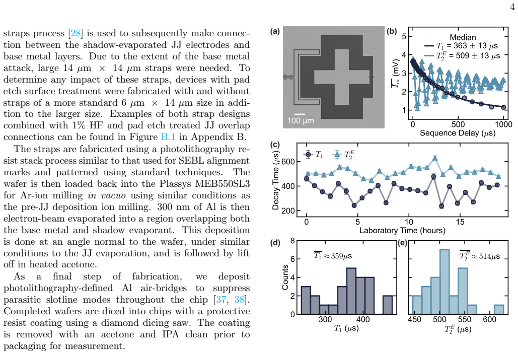
Pith's one-line read Fluorine-based surface treatments that remove germanium residue from Josephson-junction fabrication double the median energy relaxation time of aluminum-on-silicon transmon qubits, to 334 microseconds.
desk verdict Genuinely useful process result with a real statistical caveat: wafer-level replication is not reported. read the letter →
The pith
A machine-rendered reading of the paper's core claim, the machinery that carries it, and where it could break.
The reading
What carries the argument
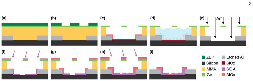
The mechanism that carries the argument is a pre-deposition surface-treatment sequence: a buffered fluorine-based pad etch (a commercial etchant containing HF, ammonium fluoride, and acetic acid with aluminum corrosion inhibitors) that strips oxide and residue from the exposed silicon at the junction footprint, followed by in-vacuo argon ion milling that cleans the surrounding silicon surface. The contamination it removes is produced by the CF$_4$ dry etch of a germanium hard mask in the suspended-bridge (Dolan-style) resist stack, whose byproducts are redeposited onto the silicon and remain trapped beneath the bridge where no line-of-sight ion mill can reach them. Materials analysis using cross-sectional scanning transmission electron microscopy with energy-dispersive X-ray and electron-energy-loss spectroscopy is the tool that identifies the germanium layer and verifies its removal.
What would settle it
Re-measure Process E on wafers after correcting the junction oxidation dose so that all 48 qubits meet frequency targets, and include every qubit in the median; if the all-inclusive median $Q$ drops to the process-of-record level near $3.3 \times 10^6$, the reported $2\times$ improvement is an artifact of dataset exclusion.
Extended reading notes
Core claim
The central claim is that the loss limiting these fixed-frequency transmons is dominated by a contamination layer at the silicon-aluminum interface under the Josephson junction, and that this layer originates as germanium dry-etch byproducts from the Ge/MMA resist stack used to form the suspended shadow-evaporation mask. Cross-sectional STEM with EDS and EELS shows a germanium-bearing layer at that interface in untreated devices, absent after pad etch plus argon ion mill; top-down SEM of removed masks shows residue under the bridge that only the wet etch can reach, and residue on the open silicon that the ion mill removes. The authors attribute the measured $2\times$ improvement in median $Q$ ($6.6 \times 10^6$ versus $3.3 \times 10^6$) to removal of this residue, and note that removing the strap connections between junction leads and base metallization gives an additional significant improvement once the interface is clean.
Load-bearing premise
The reported $2\times$ improvement assumes that qubits excluded from the $T_1$ dataset, including those with low-$J_c$ frequency targeting or calibration failures that were more common on treated wafers, are not systematically worse than the qubits that were included.
Editorial extensions
If this is right
- Other groups fabricating Al/AlOx/Al transmons with germanium-based shadow masks can apply the same pad-etch step without changing junction geometry, base metal, or oxidation parameters, and should expect a similar reduction in sub-junction interface loss.
- Because the ion mill regrows a sub-junction oxide yet the pad-etch-plus-mill process still wins, the dominant loss before treatment was the contaminant layer rather than the oxide itself; future work can target the residue directly.
- Eliminating strap connections adds a further significant quality-factor improvement once the interface is cleaned, pointing to strap processing as the next interface-loss bottleneck.
- Combining device-level $T_1$ statistics with STEM, EDS, and EELS metrology provides a template for attributing qubit decoherence to specific fabrication residues.
Reading between the lines
- If interface cleaning is the true cause, then a direct test would compare quality factors on wafers whose mask stack contains no germanium at all: the pad-etch step should then produce a much smaller improvement, since the presumed contaminant would never be introduced.
- The authors report that low-$J_c$ frequency targeting and calibration failures were more common on treated wafers; a testable prediction is that correcting the junction oxidation parameters restores target frequencies without erasing the $Q$ gain, removing the current yield penalty.
- Because pad etch attacks exposed aluminum only mildly, similar buffered-fluoride chemistries may be adaptable to niobium- or tantalum-base qubit processes, where sub-junction interfaces are also suspected loss sources.
- The observation that $T_2^E$ stays well below the $2T_1$ limit suggests that once relaxation improves to $334\,\mu\mathrm{s}$, dephasing from residual resonator photons or two-level-system dynamics will become the next bottleneck; the paper does not resolve this channel.
Editorial analysis
A structured set of objections, weighed in public.
Referee Report
Summary. This manuscript reports an empirical study of fluorine-based wet surface treatments (dilute HF and a commercial aluminum pad etch) applied to the silicon substrate surface immediately before Josephson-junction deposition in Al-based transmon qubits. Six process splits are compared across a dataset of 182 measured qubits. The central claim is that the combination of pad-etch surface treatment, pre-Junction Ar ion milling, and no strap connections (Process E) improves the median qubit quality factor by roughly 2x over the process of record (median Q = 6.6e6 and T1 = 334 us for E versus Q = 3.3e6 and T1 = 157 us for POR). Supporting materials characterization including STEM, EDS, EELS, and SEM is used to identify germanium-containing residues under the Dolan bridge that arise from the Ge-based shadow-mask dry etch, and to argue that the pad etch removes these residues, thereby reducing a dominant loss channel at the metal-substrate interface underneath the Josephson junction.
Significance. If the central claim holds, the paper identifies a specific, previously underappreciated fabrication-induced loss source (germanium dry-etch byproducts under the Dolan bridge) and demonstrates a simple, manufacturable process modification that more than doubles median transmon energy relaxation time. The study is notable for its scale (182 qubits), for combining device-level coherence statistics with independent materials analysis (STEM/EDS/EELS), and for transparently reporting which qubits were excluded from the analysis. However, the statistical case for the 2x improvement rests on qubit-level p-values from a Tukey-Kramer test applied to wafer-level process splits, and the paper does not report the number of wafers underlying each split. This missing replication information is the main load-bearing weakness; the exclusion pattern of qubits is a second, smaller concern. The materials-science narrative is internally consistent and the attributed mechanism is plausible, but the current statistical framing does not fully rule out wafer-level batch effects as an alternative explanation for part or all of the observed difference.
major comments (3)
- [Section IV A, Table I, Appendix C] The central statistical claim (2x improvement, statistically significant) is based on a Tukey-Kramer HSD test that treats each measured qubit as an independent observation, but the process conditions being compared are applied at wafer scale before dicing. The manuscript does not report the number of wafers per process split. If each split is represented by only one or two wafers, then wafer-to-wafer variability in Jc targeting, oxidation conditions, evaporator state, or handling is fully confounded with the treatment, and the qubit-level p-values substantially overstate the significance of the treatment effect. Please report the number of wafers per split and either perform a wafer-level or mixed-effects analysis, or provide evidence (e.g., between-wafer scatter within a split) that wafer-to-wafer variability is negligible relative to the observed 2x effect.
- [Section IV A] The exclusion of qubits from the T1 dataset is acknowledged, but the manuscript states that low-Jc frequency targeting and calibration failures were 'more common on wafers with pre-JJ deposition surface treatments.' Since the excluded fraction is higher in treated splits (e.g., 6/48 in Process E, larger fractions in HF splits), and since low-Jc or miscalibrated qubits could plausibly have different (typically worse) coherence properties, the reported medians may be biased upward. The sentence 'we have no evidence that this is correlated with the coherence improvements' is not a substitute for a quantitative sensitivity analysis. Please provide per-wafer exclusion counts, the frequency distributions of excluded qubits, and a robustness check (e.g., reassigning excluded qubits to low percentiles) to show that the 2x median improvement survives reasonable worst-case assumptions.
- [Table C.1 and Table I] The Tukey-Kramer HSD test compares group means, while Table I reports medians and quartiles. With skewed T1/Q distributions, a statistically significant difference in means does not directly establish the claimed difference in medians, and the p-values do not quantify the 2x median improvement that is the headline claim. Please either report mean-based comparisons alongside the medians or replace the test with a nonparametric comparison (e.g., Wilcoxon/Mann-Whitney) and state unambiguously whether the '2x improvement' statement refers to medians or means.
minor comments (5)
- [Abstract and Section II] The abstract states the surface treatments are applied 'with no other changes to the overall process flow,' but the paper actually varies the presence and size of strap connections across splits. Please qualify this statement to avoid overstating the controlled nature of the comparison.
- [Table I] The footnote for 'Qubits Measured' is defined only in Section IV A; including a brief definition in the table caption would improve readability.
- [Appendix C] The sentence 'P-values of less than 0.05 represent a rejection of the null hypothesis of equal means' is repeated in the caption; please trim redundancy and state the test assumptions explicitly.
- [Section IV B, Figure 6] The EELS discussion correctly notes that Ga contamination can produce a false Ge signal, but the statement that the Ge signal in Figure 6b is genuine because 'no corresponding Ga signal is present at that position' would benefit from showing the Ga profile in the same figure or panel for direct comparison.
- [Section III] The paper does not report the number of cooldowns or refrigerators used for each process split. Since the dataset was acquired over multiple cooldowns and four test setups, a sentence on whether process splits were balanced across measurement setups would help rule out systematic measurement drift as a confound.
Circularity Check
No circular derivation: the reported coherence improvement is a direct empirical comparison of measured qubit quality factors across process splits, with no fitted parameter, self-citation chain, or definitional identity producing the result.
full rationale
The paper makes no predictive or first-principles derivation that could collapse into its inputs. The central quantity, Q = omega_q * T1, is a direct definition of the measured quality factor, and T1 is measured with standard pulse-probe techniques; the comparison between Process E and POR is an empirical comparison of measured distributions, not a fitted prediction. The statistical test (Tukey-Kramer HSD) is applied to the measured qubit-level quality factors, and the p-values in Table C.1 are computed from those measurements rather than from any model parameter fitted to the outcome. The materials characterization (STEM, EDS, EELS, SEM) is independent of the qubit measurements and is used to propose a mechanism, not to define the reported improvement. No load-bearing result is justified solely by a self-citation: the cited prior work on Ge-based resist stacks [32], high-coherence qubits [4,33], and strap connections [28] provides fabrication context and expected effects, but the improvement claim rests on the in-paper measurements. The acknowledged exclusions of some qubits from the T1 dataset and the possibility of wafer-level confounding are data-interpretation and statistical-replication concerns, not circularity: they do not make the reported median equal to an input by construction. The paper is therefore self-contained with respect to the claimed empirical comparison, and no circular step is present.
Assumptions & free parameters
assumptions (3)
- domain assumption Q = omega_q * T1 is frequency-independent across the 3-3.5 GHz qubit range and reflects the underlying average material loss tangent.
- domain assumption Interface dielectric losses, modeled as two-level systems, dominate transmon decoherence in the device geometry studied.
- standard math The Tukey-Kramer HSD test assumptions of approximate normality and variance homogeneity hold for the quality-factor distributions.
Cite this review
Pith. "Pith review of Improving Transmon Qubit Performance with Fluorine-based Surface Treatments." pith.science (2026). https://pith.science/paper/TJ3KXACV
@misc{pith2026250708089,
  author       = {Pith},
  title        = {Pith review of: Improving Transmon Qubit Performance with Fluorine-based Surface Treatments},
  year         = {2026},
  howpublished = {\url{https://pith.science/paper/TJ3KXACV}},
  note         = {Machine review of arXiv:2507.08089}
}
abstract
Reducing materials and processing-induced decoherence is critical to the development of utility-scale quantum processors based on superconducting qubits. Here we report on the impact of two fluorine-based wet etches, which we use to treat the silicon surface underneath the Josephson junctions (JJs) of fixed-frequency transmon qubits made with aluminum base metallization. Using several materials analysis techniques, we demonstrate that these surface treatments can remove germanium residue introduced by our JJ fabrication with no other changes to the overall process flow. These surface treatments result in significantly improved energy relaxation times for the highest performing process, with median $T_1=334~\mu$s, corresponding to quality factor $Q=6.6\times10^6$. This result suggests that the metal-substrate interface directly underneath the JJs was a major contributor to microwave loss in these transmon qubit circuits prior to integration of these surface treatments. Furthermore, this work illustrates how materials analysis can be used in conjunction with quantum device performance metrics to improve performance in superconducting qubits.
Figures

Figures from the paper (4 more)


Forward citations
Cited by 1 Pith paper
-
Krypton-sputtered tantalum films for scalable high-performance quantum devices
Krypton-sputtered tantalum forms the desired BCC phase on silicon at 200°C with state-of-the-art microwave performance in resonators and qubits.
Reference graph
Works this paper leans on
-
[1]
M. Kjaergaard, M. E. Schwartz, J. Braum¨ uller, P. Krantz, J. I.-J. Wang, S. Gustavsson, and W. D. Oliver, Superconducting Qubits: Current State of Play, Annual Review of Condensed Matter Physics 11, 369 (2020), eprint: https://doi.org/10.1146/annurev- conmatphys-031119-050605
doi:10.1146/annurev- 2020
-
[2]
Y. Sung, L. Ding, J. Braum¨ uller, A. Veps¨ al¨ ainen, B. Kan- nan, M. Kjaergaard, A. Greene, G. O. Samach, C. Mc- Nally, D. Kim, A. Melville, B. M. Niedzielski, M. E. Schwartz, J. L. Yoder, T. P. Orlando, S. Gustavsson, and W. D. Oliver, Realization of High-Fidelity CZ and $ZZ$-Free iSW AP Gates with a Tunable Coupler, Phys- ical Review X 11, 021058 (202...
work page 2021
-
[3]
V. Neg ˆ ırneac, H. Ali, N. Muthusubramanian, F. Bat- tistel, R. Sagastizabal, M. Moreira, J. Marques, W. Vlothuizen, M. Beekman, C. Zachariadis, N. Haider, A. Bruno, and L. DiCarlo, High-Fidelity Controlled- $Z$ Gate with Maximal Intermediate Leakage Operating at the Speed Limit in a Superconducting Quantum Proces- sor, Physical Review Letters 126, 22050...
work page 2021
-
[4]
L. Ding, M. Hays, Y. Sung, B. Kannan, J. An, A. Di Paolo, A. H. Karamlou, T. M. Hazard, K. Azar, D. K. Kim, B. M. Niedzielski, A. Melville, M. E. Schwartz, J. L. Yoder, T. P. Orlando, S. Gustavs- son, J. A. Grover, K. Serniak, and W. D. Oliver, High-Fidelity, Frequency-Flexible Two-Qubit Fluxonium Gates with a Transmon Coupler, Physical Review X 13, 03103...
work page 2023
-
[5]
H. Zhang, C. Ding, D. Weiss, Z. Huang, Y. Ma, C. Guinn, S. Sussman, S. P. Chitta, D. Chen, A. A. Houck, J. Koch, and D. I. Schuster, Tunable Inductive Coupler for High- Fidelity Gates Between Fluxonium Qubits, PRX Quan- tum 5, 020326 (2024), publisher: American Physical So- ciety
work page 2024
-
[6]
R. Li, K. Kubo, Y. Ho, Z. Yan, Y. Nakamura, and H. Goto, Realization of High-Fidelity CZ Gate based on a Double-Transmon Coupler (2024), arXiv:2402.18926 [physics, physics:quant-ph]
work page Pith review arXiv 2024
-
[7]
W. D. Oliver and P. B. Welander, Materials in supercon- ducting quantum bits, MRS Bulletin 38, 816 (2013)
work page 2013
-
[8]
C. M¨ uller, J. H. Cole, and J. Lisenfeld, Towards under- standing two-level-systems in amorphous solids: insights from quantum circuits, Reports on Progress in Physics 82, 124501 (2019), publisher: IOP Publishing
work page 2019
Show all 52 references
-
[9]
Siddiqi, Engineering high-coherence superconducting qubits, Nature Reviews Materials 6, 875 (2021), pub- lisher: Nature Publishing Group
I. Siddiqi, Engineering high-coherence superconducting qubits, Nature Reviews Materials 6, 875 (2021), pub- lisher: Nature Publishing Group
2021
-
[10]
J. Koch, T. M. Yu, J. Gambetta, A. A. Houck, D. I. Schuster, J. Majer, A. Blais, M. H. Devoret, S. M. Girvin, and R. J. Schoelkopf, Charge-insensitive qubit design de- rived from the Cooper pair box, Physical Review A 76, 042319 (2007), publisher: American Physical Society
2007
-
[11]
V. E. Manucharyan, J. Koch, L. I. Glazman, and M. H. Devoret, Fluxonium: Single Cooper-Pair Circuit Free of Charge Offsets, Science 326, 113 (2009), publisher: American Association for the Advancement of Science Section: Report
2009
-
[12]
Bruno, G
A. Bruno, G. de Lange, S. Asaad, K. L. van der En- den, N. K. Langford, and L. DiCarlo, Reducing intrinsic loss in superconducting resonators by surface treatment and deep etching of silicon substrates, Applied Physics Letters 106, 10.1063/1.4919761 (2015), publisher: AIP Publishing
2015 doi
-
[13]
Gr¨ unhaupt, N
L. Gr¨ unhaupt, N. Maleeva, S. T. Skacel, M. Calvo, F. Levy-Bertrand, A. V. Ustinov, H. Rotzinger, A. Mon- fardini, G. Catelani, and I. M. Pop, Loss Mechanisms and Quasiparticle Dynamics in Superconducting Microwave Resonators Made of Thin-Film Granular Aluminum, Physical Revi...
2018
-
[14]
A. P. M. Place, L. V. H. Rodgers, P. Mundada, B. M. Smitham, M. Fitzpatrick, Z. Leng, A. Premkumar, J. Bryon, A. Vrajitoarea, S. Sussman, G. Cheng, T. Mad- havan, H. K. Babla, X. H. Le, Y. Gang, B. J¨ ack, A. Gye- nis, N. Yao, R. J. Cava, N. P. de Leon, and A. A. Houck, New ma...
2021
-
[15]
M. V. P. Alto´ e, A. Banerjee, C. Berk, A. Hajr, A. Schwartzberg, C. Song, M. Alghadeer, S. Aloni, M. J. Elowson, J. M. Kreikebaum, E. K. Wong, S. M. Griffin, S. Rao, A. Weber-Bargioni, A. M. Minor, D. I. Santiago, S. Cabrini, I. Siddiqi, and D. F. Ogletree, Localization and M...
2022
-
[16]
M. Bal, A. A. Murthy, S. Zhu, F. Crisa, X. You, Z. Huang, T. Roy, J. Lee, D. van Zanten, R. Pilipenko, I. Nekrashevich, D. Bafia, Y. Krasnikova, C. J. Kopas, E. O. Lachman, D. Miller, J. Y. Mutus, M. J. Reagor, H. Cansizoglu, J. Marshall, D. P. Pappas, K. Vu, K. Ya- davalli, J...
2023 arXiv
-
[17]
Bizn´ arov´ a, A
J. Bizn´ arov´ a, A. Osman, E. Rehnman, L. Chayanun, C. Kriˇ zan, P. Malmberg, M. Rommel, C. Warren, P. Dels- ing, A. Yurgens, J. Bylander, and A. Fadavi Roudsari, Mitigation of interfacial dielectric loss in aluminum-on- silicon superconducting qubits, npj Quantum Informa- ti...
2024
-
[18]
Ganjam, Y
S. Ganjam, Y. Wang, Y. Lu, A. Banerjee, C. U. Lei, L. Krayzman, K. Kisslinger, C. Zhou, R. Li, Y. Jia, M. Liu, L. Frunzio, and R. J. Schoelkopf, Surpassing mil- lisecond coherence in on chip superconducting quantum memories by optimizing materials and circuit design, Na- ture ...
2024
-
[19]
G. J. Dolan, Offset masks for lift-off photoprocessing, Ap- plied Physics Letters 31, 337 (1977)
1977
-
[20]
Lecocq, I
F. Lecocq, I. M. Pop, Z. Peng, I. Matei, T. Crozes, T. Fournier, C. Naud, W. Guichard, and O. Buisson, Junction fabrication by shadow evaporation without a suspended bridge, Nanotechnology 22, 315302 (2011). 12
2011
-
[21]
Bilmes, S
A. Bilmes, S. Volosheniuk, A. V. Ustinov, and J. Lisen- feld, Probing defect densities at the edges and in- side Josephson junctions of superconducting qubits, npj Quantum Information 8, 1 (2022), number: 1 Publisher: Nature Publishing Group
2022
-
[22]
N. S. Smirnov, E. A. Krivko, A. A. Solovieva, A. I. Ivanov, and I. A. Rodionov, Wiring surface loss of a su- perconducting transmon qubit (2023), arXiv:2311.16794 [cond-mat, physics:quant-ph]
2023 arXiv
-
[23]
J. M. Martinis, K. B. Cooper, R. McDermott, M. Stef- fen, M. Ansmann, K. D. Osborn, K. Cicak, S. Oh, D. P. Pappas, R. W. Simmonds, and C. C. Yu, Decoherence in Josephson Qubits from Dielectric Loss, Physical Review Letters 95, 210503 (2005), publisher: American Physical Society
2005
-
[24]
Wenner, R
J. Wenner, R. Barends, R. C. Bialczak, Y. Chen, J. Kelly, E. Lucero, M. Mariantoni, A. Megrant, P. J. J. O’Malley, D. Sank, A. Vainsencher, H. Wang, T. C. White, Y. Yin, J. Zhao, A. N. Cleland, and J. M. Martinis, Surface loss simulations of superconducting coplanar waveguide ...
2011
-
[25]
C. Wang, C. Axline, Y. Y. Gao, T. Brecht, Y. Chu, L. Frunzio, M. H. Devoret, and R. J. Schoelkopf, Sur- face participation and dielectric loss in superconducting qubits, Applied Physics Letters 107, 162601 (2015)
2015
-
[26]
Calusine, A
G. Calusine, A. Melville, W. Woods, R. Das, C. Stull, V. Bolkhovsky, D. Braje, D. Hover, D. K. Kim, X. Miloshi, D. Rosenberg, A. Sevi, J. L. Yoder, E. Dauler, and W. D. Oliver, Analysis and mitigation of interface losses in trenched superconducting coplanar waveguide resonator...
2018
-
[27]
Woods, G
W. Woods, G. Calusine, A. Melville, A. Sevi, E. Golden, D. Kim, D. Rosenberg, J. Yoder, and W. Oliver, De- termining Interface Dielectric Losses in Superconducting Coplanar-Waveguide Resonators, Physical Review Ap- plied 12, 014012 (2019), publisher: American Physical Society
2019
-
[28]
Dunsworth, A
A. Dunsworth, A. Megrant, C. Quintana, Z. Chen, R. Barends, B. Burkett, B. Foxen, Y. Chen, B. Chiaro, A. Fowler, R. Graff, E. Jeffrey, J. Kelly, E. Lucero, J. Y. Mutus, M. Neeley, C. Neill, P. Roushan, D. Sank, A. Vainsencher, J. Wenner, T. C. White, and J. M. Mar- tinis, Char...
2017
-
[29]
Mamin, E
H. Mamin, E. Huang, S. Carnevale, C. Rettner, N. Arel- lano, M. Sherwood, C. Kurter, B. Trimm, M. Sandberg, R. Shelby, M. Mueed, B. Madon, A. Pushp, M. Steffen, and D. Rugar, Merged-Element Transmons: Design and Qubit Performance, Physical Review Applied 16, 024023 (2021), pub...
2021
-
[30]
Verjauw, R
J. Verjauw, R. Acharya, J. Van Damme, T. Ivanov, D. P. Lozano, F. A. Mohiyaddin, D. Wan, J. Jussot, A. M. Vadiraj, M. Mongillo, M. Heyns, I. Radu, B. Govoreanu, and A. Potoˇ cnik, Path toward manufacturable supercon- ducting qubits with relaxation times exceeding 0.1 ms, npj Q...
2022
-
[31]
Van Damme, S
J. Van Damme, S. Massar, R. Acharya, T. Ivanov, D. P. Lozano, Y. Canvel, M. Demarets, D. Vangoid- senhoven, Y. Hermans, J.-G. Lai, V. Rao, M. Mongillo, D. Wan, J. De Boeck, A. Potocnik, and K. De Greve, High-coherence superconducting qubits made using industry-standard, advanc...
2024 arXiv
-
[32]
Y. N. Y. Nakamura, C. C. C. Chen, and J.-S. T. J.-S. Tsai, 100-K Operation of Al-Based Single-Electron Tran- sistors, Japanese Journal of Applied Physics 35, L1465 (1996), publisher: IOP Publishing
1996
-
[33]
F. Yan, S. Gustavsson, A. Kamal, J. Birenbaum, A. P. Sears, D. Hover, T. J. Gudmundsen, D. Rosenberg, G. Samach, S. Weber, J. L. Yoder, T. P. Orlando, J. Clarke, A. J. Kerman, and W. D. Oliver, The flux qubit revisited to enhance coherence and reproducibil- ity, Nature Communi...
2016
-
[34]
C. M. Quintana, A. Megrant, Z. Chen, A. Dunsworth, B. Chiaro, R. Barends, B. Campbell, Y. Chen, I.-C. Hoi, E. Jeffrey, J. Kelly, J. Y. Mutus, P. J. J. O’Malley, C. Neill, P. Roushan, D. Sank, A. Vainsencher, J. Wen- ner, T. C. White, A. N. Cleland, and J. M. Marti- nis, Charac...
2014
-
[35]
Chayanun, J
L. Chayanun, J. Bizn´ arov´ a, L. Zeng, P. Malmberg, A. Nylander, A. Osman, M. Rommel, P. L. Tam, E. Ols- son, P. Delsing, A. Yurgens, J. Bylander, and A. Fa- davi Roudsari, Characterization of process-related inter- facial dielectric loss in aluminum-on-silicon by resonator m...
2024
-
[36]
Dai, A maskless wet etching silicon dioxide post- CMOS process and its application, Microelectronic En- gineering Materials for Advanced Metallization (MAM 2006), 83, 2543 (2006)
C.-L. Dai, A maskless wet etching silicon dioxide post- CMOS process and its application, Microelectronic En- gineering Materials for Advanced Metallization (MAM 2006), 83, 2543 (2006)
2006
-
[37]
Rosenberg, D
D. Rosenberg, D. Kim, R. Das, D. Yost, S. Gustavsson, D. Hover, P. Krantz, A. Melville, L. Racz, G. O. Samach, S. J. Weber, F. Yan, J. L. Yoder, A. J. Kerman, and W. D. Oliver, 3D integrated superconducting qubits, npj Quantum Information 3, 42 (2017), publisher: Nature Publis...
2017
-
[38]
Rosenberg, S
D. Rosenberg, S. J. Weber, D. Conway, D.-R. W. Yost, J. Mallek, G. Calusine, R. Das, D. Kim, M. E. Schwartz, W. Woods, J. L. Yoder, and W. D. Oliver, Solid-State Qubits: 3D Integration and Packaging, IEEE Microwave Magazine 21, 72 (2020)
2020
-
[39]
Geerlings, S
K. Geerlings, S. Shankar, E. Edwards, L. Frunzio, R. J. Schoelkopf, and M. H. Devoret, Improving the quality factor of microwave compact resonators by optimizing their geometrical parameters, Applied Physics Letters 100, 192601 (2012)
2012
-
[40]
Krantz, M
P. Krantz, M. Kjaergaard, F. Yan, T. P. Orlando, S. Gus- tavsson, and W. D. Oliver, A quantum engineer’s guide to superconducting qubits, Applied Physics Reviews 6, 021318 (2019)
2019
-
[41]
J. A. Schreier, A. A. Houck, J. Koch, D. I. Schuster, B. R. Johnson, J. M. Chow, J. M. Gambetta, J. Majer, L. Frun- zio, M. H. Devoret, S. M. Girvin, and R. J. Schoelkopf, Suppressing charge noise decoherence in superconduct- ing charge qubits, Physical Review B 77, 180502 (20...
2008
-
[42]
Serniak, S
K. Serniak, S. Diamond, M. Hays, V. Fatemi, S. Shankar, L. Frunzio, R. Schoelkopf, and M. Devoret, Direct Dis- persive Monitoring of Charge Parity in Offset-Charge- Sensitive Transmons, Physical Review Applied 12, 014052 (2019), publisher: American Physical Society
2019
-
[43]
I. M. Pop, T. Fournier, T. Crozes, F. Lecocq, I. Matei, B. Pannetier, O. Buisson, and W. Guichard, Fabrication 13 of stable and reproducible submicron tunnel junctions, Journal of Vacuum Science & Technology B 30, 010607 (2012)
2012
-
[44]
Z. Chen, J. Kelly, C. Quintana, R. Barends, B. Campbell, Y. Chen, B. Chiaro, A. Dunsworth, A. Fowler, E. Lucero, E. Jeffrey, A. Megrant, J. Mutus, M. Neeley, C. Neill, P. O’Malley, P. Roushan, D. Sank, A. Vainsencher, J. Wenner, T. White, A. Korotkov, and J. M. Martinis, Measu...
2016
-
[45]
S. Yano, Y. Tarutani, H. Mori, H. Yamada, M. Hirano, and U. Kawabe, Fabrication and characteristics of NbN- based Josephson junctions for logic LSI circuits, IEEE Transactions on Magnetics 23, 1472 (1987)
1987
-
[46]
Melville, G
A. Melville, G. Calusine, W. Woods, K. Serniak, E. Golden, B. M. Niedzielski, D. K. Kim, A. Sevi, J. L. Yoder, E. A. Dauler, and W. D. Oliver, Comparison of di- electric loss in titanium nitride and aluminum supercon- ducting resonators, Applied Physics Letters 117, 124004 (2020)
2020
-
[47]
C. J. Kopas, D. P. Goronzy, T. Pham, C. G. Torres Cas- tanedo, M. Cheng, R. Cochrane, P. Nast, E. Lachman, N. Z. Zhelev, A. Valli` eres, A. A. Murthy, J.-s. Oh, L. Zhou, M. J. Kramer, H. Cansizoglu, M. J. Bedzyk, V. P. Dravid, A. Romanenko, A. Grassellino, J. Y. Mu- tus, M. C....
2024
-
[48]
M. P. Bland, F. Bahrami, J. G. C. Martinez, P. H. Preste- gaard, B. M. Smitham, A. Joshi, E. Hedrick, A. Pakpour- Tabrizi, S. Kumar, A. Jindal, R. D. Chang, A. Yang, G. Cheng, N. Yao, R. J. Cava, N. P. d. Leon, and A. A. Houck, 2D transmons with lifetimes and coherence times e...
2025 arXiv
-
[49]
Colao Zanuz, Q
D. Colao Zanuz, Q. Ficheux, L. Michaud, A. Orekhov, K. Hanke, A. Flasby, M. Bahrami Panah, G. J. Nor- ris, M. Kerschbaum, A. Remm, F. Swiadek, C. Hellings, S. Laz˘ ar, C. Scarato, N. Lacroix, S. Krinner, C. Eich- ler, A. Wallraff, and J.-C. Besse, Mitigating losses of su- perc...
2025
-
[50]
V. Savu, J. Kivioja, J. Ahopelto, and J. Brugger, Quick and Clean: Stencil Lithography for Wafer-Scale Fabrica- tion of Superconducting Tunnel Junctions, IEEE Trans- actions on Applied Superconductivity 19, 242 (2009), conference Name: IEEE Transactions on Applied Super- conductivity
2009
-
[51]
P. B. Welander, V. Bolkhovsky, T. J. Weir, M. A. Gouker, and W. D. Oliver, Shadow evaporation of epi- taxial Al/Al2O3/Al tunnel junctions on sapphire utiliz- ing an inorganic bilayer mask (2012), arXiv:1203.6007 [cond-mat]
2012 arXiv
-
[52]
Tsioutsios, K
I. Tsioutsios, K. Serniak, S. Diamond, V. V. Sivak, Z. Wang, S. Shankar, L. Frunzio, R. J. Schoelkopf, and M. H. Devoret, Free-standing silicon shadow masks for transmon qubit fabrication, AIP Advances 10, 065120 (2020), publisher: American Institute of Physics
2020
Reviewed August 6, 2026 · model on record in the stance chip above.
Discussion (0). Continue with ORCID to comment.