REVIEW 3 major objections 5 minor 3 references
Innovative Oxide Transistor Satisfying Performance and Reliability Simultaneously by Understanding of Physics and Materials Properties
T0 review · 3 major / 5 minor · reviewed 2026-08-04 · deepseek-v4-flash
Pith's one-line read An IGZO transistor uncouples speed from stress stability by giving the channel and the contacts different oxide thicknesses.
desk verdict A genuinely new access-resistance decoupling structure, but the 'breaks the reliability constraint' headline needs post-stress performance data before it sticks. read the letter →
The pith
A machine-rendered reading of the paper's core claim, the machinery that carries it, and where it could break.
The reading
What carries the argument
The central mechanism is a deliberately non-uniform channel: a thick oxide capping over the channel body and a thin oxide layer in the source-drain contact regions. This splits the two roles that previously fell on a single film thickness: the thin contact region minimizes the thickness-dependent access resistance racss that limits on-current and extrinsic mobility in staggered structures, while the thick channel capping suppresses the surface donor band-tail states that positive bias stress generates and that cause Vt shifts and a third, non-ideal conducting path. The analysis is carried by a multi-channel equivalent circuit—accumulation channel, bulk channel, and possible damaged surface c
What would settle it
Fabricate the Addition-flow device without the thick IGZO cap but with the same thin contact region: if the Vt shift stays near 15 mV the cap is not doing the work, and if it returns to volts the surface-passivation story is confirmed. Separately, stress the 10 nm-contact device at 400°C thermal budget and measure PBS again: the paper shows no elevated-temperature or post-anneal reliability data, so preserving ~15 mV there would be the decisive test for VLSI/BEOL claims.
Extended reading notes
Core claim
On the paper's own terms, the central discovery is that the performance–reliability tradeoff in IGZO transistors is structural, not a materials limit. The paper identifies two coexisting channels in an accumulation-mode oxide transistor—the surface accumulation channel and the bulk film channel—and an access-resistance component that grows with channel thickness because current must travel from top source-drain contacts down to the bottom gate interface. It then shows that bias-stress degradation is driven by the oxide surface/back channel, so a thick channel suppresses the damage but a thin channel is needed for low access resistance. The proposed 'innovative transistor' separates the two r
Load-bearing premise
The central claim stands on the assumption that positive-bias-stress damage is a surface effect in the oxide channel, so a thick channel cap suppresses it while the thin contact regions under the source and drain do not themselves create new instability; the paper states the PBS mechanism as speculation, and all reliability data are room-temperature shadow-mask measurements.
Editorial extensions
If this is right
- Extrinsic mobility approaches the intrinsic IGZO mobility since the thin contact region removes the thickness-dependent access resistance; a 5 nm contact version reaches 22 cm2/Vs.
- PBS-induced Vt shift drops from a few volts in a conventional thin IGZO transistor to 15 mV at 10 nm contact thickness, with zero hysteresis, so the structure satisfies performance and reliability in the same device.
- Both the Addition and Subtraction process flows produce the same zero-hysteresis, high-current behavior, indicating the benefit comes from the geometry rather than from a specific deposition or etch step.
- The multi-channel TLM interpretation converts apparent negative contact resistance into a diagnostic for surface damage, giving a way to detect plasma or processing damage in thin-oxide devices.
- The modified coplanar idea—depositing channel material before the ITO contacts and locally inserting high-carrier-concentration material in the SD region—offers additional freedom to reduce contact resistance without degrading subthreshold slope or on/off ratio.
Reading between the lines
- If the surface donor band-tail mechanism is correct, the same thick-cap/thin-contact split should also reduce other surface-mediated instabilities, such as elevated-temperature bias-temperature instability and negative-bias illumination stress—regimes the paper does not report.
- The 15 mV reliability number is demonstrated only at room temperature on shadow-mask devices with 50 nm SiO2 and p+Si gates; the paper's own coplanar ITO data degrade at 400°C, so holding 15 mV through a realistic BEOL thermal budget is a testable extension, not yet a demonstrated one.
- A direct measurement of the hypothesized donor band-tail states—for example, stress-induced changes in subthreshold swing, low-frequency noise, or optical absorption—would convert the paper's speculation into a verified mechanism.
- The thin-contact design may also change how effective channel length is extracted from short-channel TLM, since the third-channel and channel-shortening effects would be suppressed; this is a metrological consequence the authors do not develop.
Editorial analysis
A structured set of objections, weighed in public.
Referee Report
Summary. The paper reviews accumulation-mode oxide-transistor physics and materials properties, identifies a thickness trade-off between performance (thinner channels give higher on-current) and reliability (thicker channels give better positive-bias-stress stability), and proposes a transistor architecture with a thick channel capping region and thin channel contact regions. Using shadow-mask fabricated IGZO transistors, the authors report an extrinsic mobility of 20 cm2/Vs, near-zero hysteresis, and a 15 mV Vt shift after PBS at 3 MV/cm for 1000 s at room temperature, claiming this breaks the performance/reliability constraint of conventional IGZO transistors.
Significance. If the demonstrated result is robust, it would provide a practical structural route to combine high drive current and PBS stability in oxide transistors, relevant to high-resolution displays and BEOL-compatible oxide electronics. The paper contains systematic materials characterization (R-T, XRD), a clear discussion of process-damage effects, and a useful analysis of access resistance in staggered versus coplanar structures. The proposal of Addition and Subtraction process flows, both showing zero hysteresis, is a concrete engineering contribution. However, the reliability claim currently rests on a single Vt-shift measurement with no post-stress performance metrics, and the invoked degradation mechanism is explicitly speculative. Thus the work is a promising demonstration rather than an established breakthrough.
major comments (3)
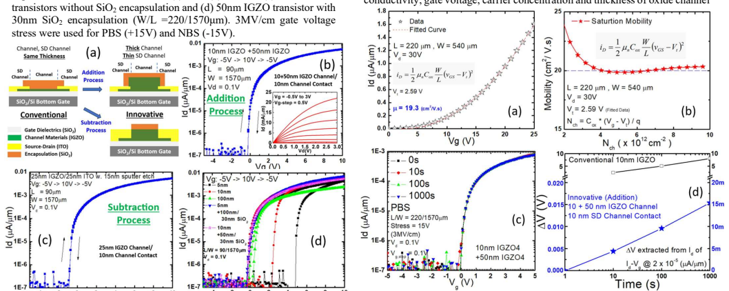
- [INNOVATIVE TRANSISTOR AND PROCESS, Fig. 14(c,d)] The PBS reliability demonstration reports only the pre/post Vt shift. No post-stress on-current, saturation mobility, subthreshold swing, or contact resistance are given. This is a load-bearing omission because the thin 10 nm channel-contact regions sit in the thickness regime where Fig. 10 shows stress-induced apparent negative contact resistance in 5 nm IGZO and Fig. 11 shows large PBS shifts. If the thin contact regions degrade under stress, Vt could remain stable while on-current/mobility degrade through increased series resistance, so the claim of satisfying performance and reliability simultaneously is not established. Please provide full transfer curves before and after stress with extracted parameters, and ideally TLM data after stress.
- [INNOVATIVE TRANSISTOR AND PROCESS, Fig. 14(d)] The baseline for the PBS comparison is described only as 'an IGZO control device' with 'a few volts' shift. It is not stated whether this control is a conventional 10 nm IGZO transistor with or without SiO2 encapsulation. Since the paper itself shows that SiO2 encapsulation alone reduces the 50 nm IGZO PBS shift from several volts to 50 mV (Fig. 11(d)), the comparison must use the same passivation stack as the innovative device to support the claim that the structure, not simply the capping, breaks the thickness trade-off. Report PBS for conventional 10 nm and 50 nm IGZO transistors with the same 50 nm channel capping as the Addition process.
- [THICKNESS DEPENDENT ELECTRIC PROPERTIES, Fig. 12] The mechanism for the PBS improvement is explicitly speculative: 'It is speculated that PBS would cause a positively charged donor band tail states on the surface oxide channel.' The third non-ideal channel is inferred from the same TLM and stress data that it is then used to explain, making that part of the interpretation circular. The empirical device claim does not depend on this mechanism, but the paper's conceptual claim of 'Understanding of Physics' and the assumption that the thin contact regions do not introduce a new instability do. Please either provide direct evidence (e.g., surface-sensitive characterization or controlled surface treatments) or clearly mark the mechanism as a hypothesis and frame the reliability claim as device-level only.
minor comments (5)
- [Abstract] The stress condition '3 MV/cm stress for 1000s' should specify the polarity (positive gate bias) and the corresponding gate voltage (+15 V for 50 nm SiO2). Also, the unit 'cm2V-1s-1' should be typeset as cm^2 V^-1 s^-1.
- [Fig. 11 caption] The caption lists PBS/NBS results for (a) 200, (b) 50, and (c) 10 nm IGZO without encapsulation and (d) 50 nm IGZO with 30 nm SiO2 encapsulation. Please clarify in the text whether the same stress condition (3 MV/cm, 1000 s, RT) applies to all panels, and whether the encapsulated device in (d) uses the same process flow as the innovative device.
- [Fig. 14(a,b)] The mobility extraction is stated as 'from the saturation region' but no equation or definition of Vt and channel dimensions is provided. Include the extraction formula and the W/L values used, so the 20 cm2/Vs value is reproducible.
- [References] Reference [5] is incomplete: it lacks the paper title and appears as 'S.H. Rha, ", IEEE Trans. On Electron Devices...'. Also, reference formatting is inconsistent across [1]-[5].
- [General] There is no statistical information on device-to-device variation. The headline values (20 cm2/Vs, 15 mV, zero hysteresis) appear to come from single exemplars. Adding the number of measured devices, mean values, and spread would strengthen the claims.
Circularity Check
No significant circularity: the central claims are measured device results, and the proposed mechanisms are post-hoc interpretations rather than inputs used to derive the measurements.
full rationale
The paper's central claims—high extrinsic mobility (20 cm2V-1s-1) and 15 mV PBS Vt shift for the innovative 10 nm IGZO transistor—are experimental measurements on fabricated shadow-mask devices, not quantities derived from an assumed model. The 'third non-ideal channel' and PBS-induced donor band-tail states are explicitly speculative ('It is speculated that PBS would cause a positively charged donor band tail states on the surface oxide channel') and are offered as interpretations of observed TLM and stress data, not as fitted inputs that then 'predict' the same data. No parameter is fitted to a subset and then renamed a prediction, and no load-bearing step reduces by construction to its own input. The cited reference [5] is external prior work on negative contact resistance, not a self-citation chain. The reliability claim's incompleteness (only Vt shift reported, room-temperature shadow-mask devices) is a correctness/evidence concern, not circularity. Therefore no circular step can be exhibited, and the appropriate score is 0.
Assumptions & free parameters
assumptions (3)
- domain assumption Oxide FETs have two conducting channels, an accumulation channel at the gate interface and a bulk film channel, and both contribute to current.
- ad hoc to paper Positive bias stress creates positively charged donor band tail states on the oxide channel surface, producing a third non-ideal current path and Vt shift.
- domain assumption SiO2 encapsulation passivates the oxide channel surface and reduces Vt shifts.
invented entities (2)
-
Third non-ideal surface channel
-
PBS-induced positively charged donor band tail states
Cite this review
Pith. "Pith review of Innovative Oxide Transistor Satisfying Performance and Reliability Simultaneously by Understanding of Physics and Materials Properties." pith.science (2026). https://pith.science/paper/DT7HD6XC
@misc{pith2026250907886,
  author       = {Pith},
  title        = {Pith review of: Innovative Oxide Transistor Satisfying Performance and Reliability Simultaneously by Understanding of Physics and Materials Properties},
  year         = {2026},
  howpublished = {\url{https://pith.science/paper/DT7HD6XC}},
  note         = {Machine review of arXiv:2509.07886}
}
read the original abstract
Guided by a comprehensive analysis of accumulation mode transistor physics and oxide semiconductor materials properties, we demonstrate an innovative oxide semiconductor transistor structure and process flow that break the constraint between performance and reliability observed in conventional InGaZnO4 (IGZO) transistors. The newly proposed 10 nm innovative IGZO transistor features high on-current, high extrinsic mobility (20 cm2V-1s-1), near-zero hysteresis, and only 15 mV Vt shift after positive-bias-stress (PBS) of 3 MV/cm stress for 1000s at room temperature.
Figures


Figures from the paper (5 more)


Reference graph
Works this paper leans on
-
[2]
J.-P. Colinge,IEEE Trans. On Electron Devices, Vol. 37, pp. 718-723, 1990
work page 1990
-
[3]
MIT Opencourseware, 6.012,Microelectronic device and circuits,Fall 2009. [4]W.Fichtner,IEEE Solid State Circuits and Technology Workshop on Scaling and Microlithography,New York, 1980
work page 2009
-
[5]
S.H. Rha, “, IEEE Trans. On Electron Devices, Vol. 59, pp. 3357-3363, 2012. Fig. 7. Id-Vg curves of 30nm SiO2 encapsulated staggered 5nm (a) IGZO (b) In2O3(c) ITO and (d) non-SiO2 encapsulated coplanar ITO transistors with sequential temperature ramping annealing in oxygen. Fig. 6. Sheet Resistance (Rs) and Synchrotron XRD versus temperature (T) measureme...
work page 2012
Reviewed August 4, 2026 · model on record in the stance chip above.
Discussion (0). Continue with ORCID to comment.