PALTO: Physics-Informed Active Learning for Tri-Gate FinFET Design Optimization for Vertical Power Delivery
Pith reviewed 2026-06-28 17:29 UTC · model grok-4.3
The pith
Physics-informed active learning finds GaN tri-gate FinFET designs with twice the switching efficiency of industrial benchmarks.
A machine-rendered reading of the paper's core claim, the machinery that carries it, and where it could break.
Core claim
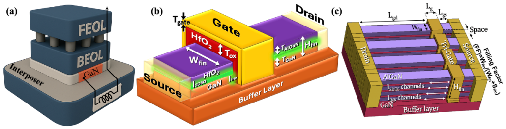
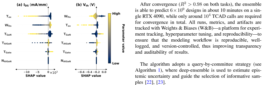
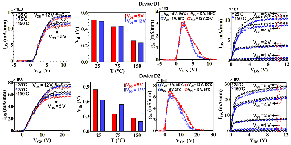
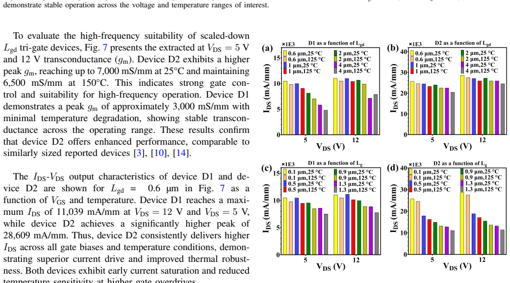
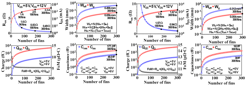
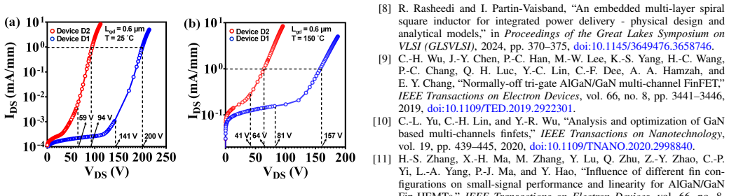
The physics-informed active learning framework identifies two normally-off GaN tri-gate FinFET configurations; in 300-fin arrays device D1 delivers 3.3 A at 0.49 ohm on-resistance with a 5 pC·ohm figure of merit that is approximately twice that of device D2, while both outperform industrial benchmarks on different metrics.
What carries the argument
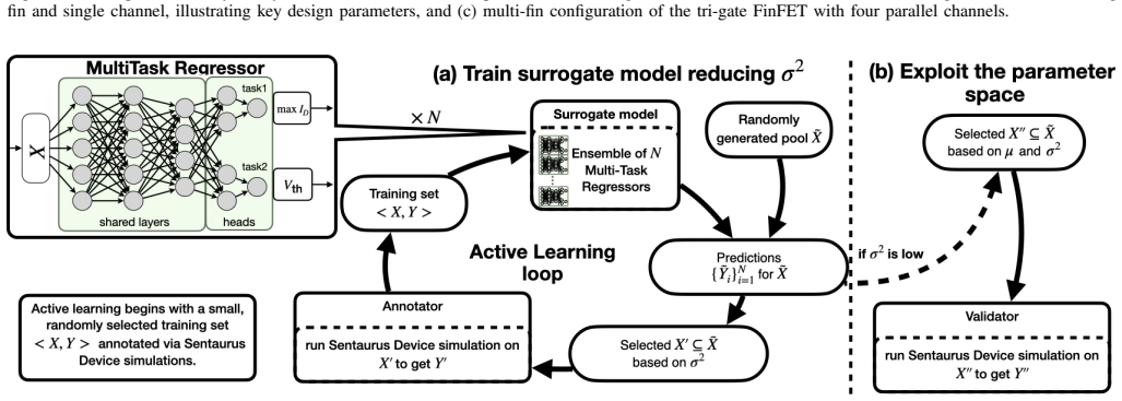
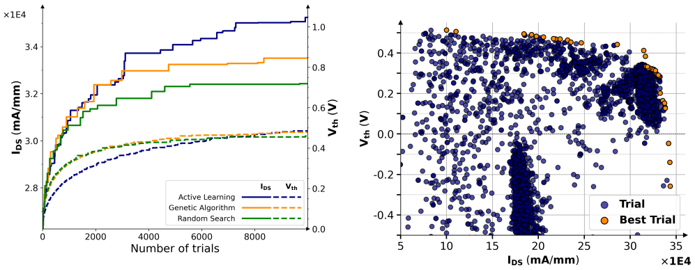
Physics-informed active learning framework that selects which TCAD simulations to run next by balancing exploration of structural parameters such as the GaN-to-AlGaN thickness ratio.
If this is right
- Device D1 achieves roughly 2 times greater switching efficiency than device D2 in application-specific metrics.
- Device D2 exhibits higher drive current in single-fin multi-channel tests but lower overall efficiency in scaled arrays.
- Both designs operate in normally-off mode and beat existing industrial devices from different performance angles.
- Aggressively scaled gate-to-drain lengths become feasible once the thickness ratio is tuned correctly.
Where Pith is reading between the lines
- The same guided-simulation approach could shorten design cycles for other wide-bandgap power transistors beyond the two devices shown.
- Vertical power delivery systems might reach higher current densities if the identified thickness-ratio optimum generalizes across process variations.
- Comparing the learned optima against fabricated prototypes would test whether the simulation-based figure of merit translates to measured efficiency gains.
Load-bearing premise
The active learning loop can converge on globally optimal device geometries without missing superior points or introducing biases from the underlying simulations.
What would settle it
An exhaustive or denser sampling of the same design space that produces a device with a figure of merit better than 5 pC·ohm would show the claimed optima are incomplete.
Figures
read the original abstract
This paper demonstrates the effectiveness of machine learning-driven optimization for designing application-specific GaN tri-gate FinFETs in vertical power delivery systems. Conventional TCAD-based approaches are computationally intensive and insufficient for navigating the high-dimensional, nonlinear design space of advanced GaN devices. To address this, a physics-informed active learning framework is used to intelligently guide simulations, accelerating convergence while preserving accuracy. This ML-guided approach enables the discovery of optimal configurations by efficiently exploring key structural parameters -- most notably the GaN-to-AlGaN thickness ratio -- a long-standing focus of debate in device design. By systematically exploring key structural parameters, two optimized devices with aggressively scaled gate-to-drain lengths are identified. Single-fin, multi-channel simulations show that device~D2, with a thinner GaN channel relative to the AlGaN barrier, achieves higher drive current. However, in a 300-fin configuration, device~D1 outperforms device~D2 by delivering 3.3\,A at 0.49~ohm on-resistance -- approximately 2$\times$ better -- despite slightly higher parasitics. Both devices operate in a normally-off mode. Based on an application-specific figure of merit, device~D1 achieves 5\,pC$\cdot$ohm, demonstrating 2$\times$ greater switching efficiency than device~D2, while both designs outperform industrial benchmarks from different performance standpoints.
Editorial analysis
A structured set of objections, weighed in public.
Referee Report
Summary. The manuscript introduces PALTO, a physics-informed active learning framework to optimize structural parameters (including GaN-to-AlGaN thickness ratio and gate-to-drain length) of tri-gate FinFETs for vertical power delivery. It claims this ML-guided approach accelerates TCAD exploration of the high-dimensional nonlinear design space while preserving accuracy, identifying two normally-off devices: D2 (thinner GaN channel) shows higher drive current in single-fin/multi-channel simulations, while D1 delivers 3.3 A at 0.49 ohm on-resistance in 300-fin configuration and achieves an application-specific figure of merit of 5 pC·ohm (claimed 2× switching efficiency over D2). Both devices are asserted to outperform industrial benchmarks from different standpoints.
Significance. If the active-learning results are shown to be robust, the work would demonstrate a practical route to reducing the computational cost of TCAD-based device optimization in GaN power electronics, with concrete performance numbers (e.g., the 5 pC·ohm FOM) that could guide application-specific design. The emphasis on the long-debated GaN-to-AlGaN ratio and the scaling from single-fin to 300-fin configurations adds relevance to vertical power delivery. However, the significance is limited by the absence of any reported validation of the surrogate model or search procedure.
major comments (2)
- [Abstract / Results] Abstract and results sections: The central claim that the physics-informed active learning identifies globally optimal D1 and D2 (underpinning the 2× efficiency and benchmark-outperformance assertions) lacks any convergence diagnostics, multiple-run statistics, query-budget analysis, or comparison against exhaustive search on a reduced subspace. In high-dimensional nonlinear TCAD landscapes this omission directly undermines the optimality guarantee.
- [Methods / Results] Methods / simulation setup: The transition from single-fin (where D2 wins) to 300-fin (where D1 wins) performance is presented without describing how the active-learning surrogate incorporates multi-fin scaling, parasitic extraction, or thermal effects; this gap is load-bearing for the application-specific FOM comparison.
minor comments (2)
- [Abstract] The abstract states 'approximately 2× better' without specifying the exact baseline metric or error bars on the 3.3 A / 0.49 ohm numbers.
- [Abstract] Notation for the figure of merit (pC·ohm) should be defined explicitly with the formula used to compute the 5 pC·ohm value.
Simulated Author's Rebuttal
We thank the referee for the detailed and constructive report. We address each major comment below, agreeing that additional documentation and analysis are needed to support the optimality claims and multi-fin evaluation workflow. Revisions will be incorporated in the next version.
read point-by-point responses
-
Referee: [Abstract / Results] Abstract and results sections: The central claim that the physics-informed active learning identifies globally optimal D1 and D2 (underpinning the 2× efficiency and benchmark-outperformance assertions) lacks any convergence diagnostics, multiple-run statistics, query-budget analysis, or comparison against exhaustive search on a reduced subspace. In high-dimensional nonlinear TCAD landscapes this omission directly undermines the optimality guarantee.
Authors: We agree that the current manuscript lacks explicit convergence diagnostics, multiple independent runs, query-budget analysis, and comparisons to exhaustive or random search. The active-learning procedure used a fixed budget guided by the physics-informed acquisition function, but without these supporting analyses the global optimality claim cannot be fully substantiated. We will revise the results section to include convergence curves of the surrogate objective, statistics from at least five independent runs with varied initial seeds, a query-budget sensitivity plot, and a comparison against random sampling on a reduced two-dimensional subspace (GaN-to-AlGaN ratio and gate-to-drain length) to demonstrate that the identified designs are robust. revision: yes
-
Referee: [Methods / Results] Methods / simulation setup: The transition from single-fin (where D2 wins) to 300-fin (where D1 wins) performance is presented without describing how the active-learning surrogate incorporates multi-fin scaling, parasitic extraction, or thermal effects; this gap is load-bearing for the application-specific FOM comparison.
Authors: The active-learning loop was performed exclusively on single-fin TCAD simulations because 300-fin device simulations are too expensive to run iteratively inside the optimization. The surrogate therefore models only single-fin electrostatics and transport; multi-fin scaling, parasitic extraction, and thermal effects were evaluated only after the active-learning stage by running full 300-fin TCAD simulations on the two candidate designs. We will revise the methods section to explicitly state this two-stage workflow, add a description of the parasitic and thermal models used in the 300-fin simulations, and include a brief discussion of how the application-specific FOM is computed from those post-optimization results. revision: yes
Circularity Check
No significant circularity; claims rest on external TCAD simulations
full rationale
The abstract presents a physics-informed active learning method to explore GaN FinFET parameter space and reports simulated performance metrics (drive current, on-resistance, figure of merit) for devices D1 and D2. No equations, fitted parameters renamed as predictions, self-definitional constructs, or load-bearing self-citations appear in the provided text. Performance numbers are stated as outputs of single-fin and 300-fin TCAD runs rather than tautological reductions to the optimization inputs. The derivation chain is therefore self-contained against external simulation benchmarks; no circular step can be quoted.
Axiom & Free-Parameter Ledger
Reference graph
Works this paper leans on
-
[1]
Vertical power delivery for high performance computing systems with buck-derived regulators,
S. Krishnakumar, M. Choi, R. R. Khorasani, R. Sharma, M. Swami- nathan, S. Kumar, and I. Partin-Vaisband, “Vertical power delivery for high performance computing systems with buck-derived regulators,” in IEEE Electronic Components and Technology Conference (ECTC), 2024, pp. 2136–2142, doi:10.1109/ECTC51529.2024.00364
-
[2]
S. Krishnakumar and I. Partin-Vaisband, “Vertical power delivery for emerging packaging and integration platforms-power conversion and dis- tribution,” inIEEE International System-on-Chip Conference (SOCC), 2023, pp. 1–6, doi:10.1109/SOCC58585.2023.10256973
-
[3]
A. Sadeghi and I. Partin-Vaisband, “Analysis and optimization of multi-channel e-mode AlGaN/GaN Trigate FinFET for vertical power delivery with embedded power converters,” inIEEE Electronic Com- ponents and Technology Conference (ECTC), 2025, pp. 1282–1289, doi:10.1109/ECTC51687.2025.00220
-
[4]
Bandit learning-driven power gating with state retention for high performance computing,
S. Abdelzaher, M. Gharib, A. R. Trivedi, and I. Partin-Vaisband, “Bandit learning-driven power gating with state retention for high performance computing,” inIEEE 34th Conference on Electrical Per- formance of Electronic Packaging and Systems (EPEPS), 2025, pp. 1–3, doi:10.1109/EPEPS63858.2025.11346621
-
[5]
R. Rasheedi and I. Partin-Vaisband, “High aspect ratio spiral inductor with progressive turn widths for embedded power converters,” inIEEE 75th Electronic Components and Technology Conference (ECTC), 2025, pp. 2271–2277, doi:10.1109/ECTC51687.2025.00386
-
[6]
An analytical model for high-frequency through silicon vias,
M. A. Gharib, S. Abdelzaher, and I. Partin-Vaisband, “An analytical model for high-frequency through silicon vias,” inProceedings of the Great Lakes Symposium on VLSI (GLSVLSI), 2024, pp. 282–286, doi:10.1145/3649476.3658792
-
[7]
M. Gharib and I. Partin-Vaisband, “Efficient scalable thermoelec- tric modeling of high-frequency cylindrical interconnects for het- erogeneous package arrays,” inIEEE 75th Electronic Compo- nents and Technology Conference (ECTC), 2025, pp. 2278–2285, doi:10.1109/ECTC51687.2025.00387
-
[8]
R. Rasheedi and I. Partin-Vaisband, “An embedded multi-layer spiral square inductor for integrated power delivery - physical design and analytical models,” inProceedings of the Great Lakes Symposium on VLSI (GLSVLSI), 2024, pp. 370–375, doi:10.1145/3649476.3658746
-
[9]
Normally-off tri-gate AlGaN/GaN multi-channel FinFET,
C.-H. Wu, J.-Y . Chen, P.-C. Han, M.-W. Lee, K.-S. Yang, H.-C. Wang, P.-C. Chang, Q. H. Luc, Y .-C. Lin, C.-F. Dee, A. A. Hamzah, and E. Y . Chang, “Normally-off tri-gate AlGaN/GaN multi-channel FinFET,” IEEE Transactions on Electron Devices, vol. 66, no. 8, pp. 3441–3446, 2019, doi:10.1109/TED.2019.2922301
-
[10]
Analysis and optimization of GaN based multi-channels finfets,
C.-L. Yu, C.-H. Lin, and Y .-R. Wu, “Analysis and optimization of GaN based multi-channels finfets,”IEEE Transactions on Nanotechnology, vol. 19, pp. 439–445, 2020, doi:10.1109/TNANO.2020.2998840
-
[11]
H.-S. Zhang, X.-H. Ma, M. Zhang, Y . Lu, Q. Zhu, Z.-Y . Zhao, C.-P. Yi, L.-A. Yang, P.-J. Ma, and Y . Hao, “Influence of different fin con- figurations on small-signal performance and linearity for AlGaN/GaN Fin-HEMTs,”IEEE Transactions on Electron Devices, vol. 66, no. 8, pp. 3302–3309, 2019, doi:10.1109/TED.2019.2921445
-
[12]
Multidimensional device architec- tures for efficient power electronics,
Y . Zhang, F. Udrea, and H. Wang, “Multidimensional device architec- tures for efficient power electronics,”Nature Electronics, vol. 5, pp. 723–734, 2022, doi:10.1038/s41928-022-00860-5
-
[13]
J. Ma, C. Erine, P. Xiang, K. Cheng, and E. Matioli, “Multi-channel tri-gate normally-on/off AlGaN/GaN MOSHEMTs on Si substrate with high breakdown voltage and low ON-resistance,”Applied Physics Let- ters, vol. 113, no. 24, p. 242102, 2018, doi:10.1063/1.5064407
-
[14]
Normally off single-nanoribbonAl 2O3/GaNMIS- FET,
K.-S. Im, R.-H. Kim, K.-W. Kim, D.-S. Kim, C. S. Lee, S. Cristoloveanu, and J.-H. Lee, “Normally off single-nanoribbonAl 2O3/GaNMIS- FET,”IEEE Electron Device Letters, vol. 34, no. 1, pp. 27–29, 2013, doi:10.1109/LED.2012.2222861
-
[15]
Tri-gate GaN junction HEMTs: Physics and performance space,
Y . Ma, M. Xiao, Z. Du, H. Wang, and Y . Zhang, “Tri-gate GaN junction HEMTs: Physics and performance space,”IEEE Transac- tions on Electron Devices, vol. 68, no. 10, pp. 4854–4861, 2021, doi:10.1109/TED.2021.3103157
-
[16]
S. Abdelzaher, M. Gharib, and I. Partin-Vaisband, “Hybrid voltage regulators for high performance computing: Analytical models and design methodology,” inIEEE Electronic Components and Technology Conference (ECTC), 2025, pp. 2286–2292, doi:10.1109/ECTC51687.2025.00388
-
[17]
Y . Xu, S. Cristoloveanu, M. Bawedin, K.-S. Im, and J.-H. Lee, “Per- formance improvement and sub-60 mV/decade swing in AlGaN/GaN FinFETs by simultaneous activation of 2DEG and sidewall MOS chan- nels,”IEEE Transactions on Electron Devices, vol. 65, no. 3, pp. 915– 920, 2018, doi:10.1109/TED.2017.2788920
-
[18]
Multi-channel nanowire de- vices for efficient power conversion,
L. Nela, J. Ma, C. Erine, P. Xiang, T.-H. Shen, V . Tileli, T. Wang, K. Cheng, and E. Matioli, “Multi-channel nanowire de- vices for efficient power conversion,”Nature Electronics, vol. 4, 2021, doi:10.1038/s41928-021-00550-8
-
[19]
J. Kwak, S. Deng, J. Lee, S. Datta, and S. Yu, “Backside active power delivery with hybrid dc–dc converter enabled by amorphous oxide semi- conductor transistors,”IEEE Transactions on V ery Large Scale Integra- tion (VLSI) Systems, pp. 1–10, 2025, doi:10.1109/TVLSI.2025.3570078
-
[20]
M. D. McKay, R. J. Beckman, and W. J. Conover, “A comparison of three methods for selecting values of input variables in the analysis of output from a computer code,”Technometrics, vol. 21, no. 2, pp. 239– 245, 1979. [Online]. Available: http://www.jstor.org/stable/1268522
arXiv 1979
-
[21]
Multi-task learning using uncertainty to weigh losses for scene geometry and semantics
R. Cipolla, Y . Gal, and A. Kendall, “Multi-task learning using uncer- tainty to weigh losses for scene geometry and semantics,” inIEEE/CVF Conference on Computer Vision and Pattern Recognition (CVPR), 2018, pp. 7482–7491, doi:10.1109/CVPR.2018.00781
-
[22]
Active learning literature survey,
B. Settles, “Active learning literature survey,” University of Wisconsin– Madison, Computer Sciences Technical Report 1648, 2009. [On- line]. Available: http://axon.cs.byu.edu/ ∼martinez/classes/778/Papers/ settles.activelearning.pdf
2009
-
[23]
Simple and scalable predictive uncertainty estimation using deep ensembles,
B. Lakshminarayanan, A. Pritzel, and C. Blundell, “Simple and scalable predictive uncertainty estimation using deep ensembles,” inProceedings of the 31st International Conference on Neural Information Processing Systems (NIPS), ser. NIPS ’17. Red Hook, NY , USA: Curran Associates Inc., 2017, pp. 6405–6416
2017
-
[24]
K. Deb, A. Pratap, S. Agarwal, and T. Meyarivan, “A fast and elitist multiobjective genetic algorithm: Nsga-ii,”IEEE Transactions on Evolutionary Computation, vol. 6, no. 2, pp. 182–197, 2002, doi:10.1109/4235.996017
discussion (0)
Sign in with ORCID, Apple, or X to comment. Anyone can read and Pith papers without signing in.