Modeling the computer memory based on the ferromagnet/superconductor multilayers
Pith reviewed 2026-05-24 22:00 UTC · model grok-4.3
The pith
Hybrid pseudospin valve and superconducting-ferromagnetic transistor cells switch in under one nanosecond while using under 100 femtojoules per operation.
A machine-rendered reading of the paper's core claim, the machinery that carries it, and where it could break.
Core claim
The model shows that memory cells built from hybrid pseudospin-valve and superconducting-ferromagnetic-transistor structures achieve ultrafast switching in sub-nanoseconds and energy consumption below 100 femtojoules per operation. Logical states are encoded in the two resistance levels of the pseudospin valve; these levels are toggled when a word pulse applied to the transistor coincides with a bit pulse on the cell, driving the transistor into its resistive state and thereby triggering orthogonal spin transfer inside the valve. The entire dynamics rests on the non-equilibrium and nonstationary properties of the two constituent devices.
What carries the argument
The PS/SFT memory cell circuit in which a three-terminal Josephson superconducting-ferromagnetic transistor controls orthogonal spin transfer inside a pseudospin valve to switch it between two resistance-defined logical states.
If this is right
- Circuits containing twelve or thirty cells exhibit the same sub-nanosecond switching and sub-100 femtojoule energy figures.
- The model framework permits direct inclusion of noise, punch-through, crosstalk, and parasitic effects.
- The cells maintain impedances of 1-30 ohms and therefore integrate with existing superconducting circuits without additional matching networks.
- Read and write operations are realized by the temporal coincidence of a word pulse on the transistor and a bit pulse on the cell.
Where Pith is reading between the lines
- Arrays larger than thirty cells could be simulated to locate the onset of thermal or fabrication-induced errors that the present model leaves unexamined.
- The same non-equilibrium dynamics might be reused to design hybrid magnetic-superconducting logic gates whose switching also relies on controlled spin transfer.
- Direct connection to Josephson-junction processors would remove the need for separate memory buses and their associated latency.
- Fabrication tolerances on the thicknesses of the ferromagnetic and superconducting layers could be tested numerically before committing to lithography runs.
Load-bearing premise
The pseudospin valve switches reliably between its two logical resistance states whenever the superconducting-ferromagnetic transistor is driven into its resistive state by overlapping word and bit pulses.
What would settle it
Measure the time and energy required for resistance to change in a fabricated single cell when word and bit pulses are applied simultaneously versus when they are applied separately.
Figures
read the original abstract
A model of superconducting computer memory exploiting the orthogonal spin transfer (OST) in the pseudospin valve (PS) that is controlled by the three-terminal Josephson superconducting-ferromagnetic transistor (SFT) is developed. The building blocks of the memory are hybrid PS and SFT structures. The memory model is formulated in terms of the equation-defined PS and SFT devices integrated into the PS/SFT memory cell (MC) circuit. Logical units "0" and "1" are associated with the two PS states respectively characterized by two different values of resistance. Elementary logical operations comprising the read/write processes occur when a word pulse applied to the SFT's injector coincides with the respective bit pulse acting on MC. Physically, a word pulse triggers SFT to a resistive state, causing the PS switching between the logical "0" and "1" states. Thus, the whole switching dynamics of MC depends on the non-equilibrium and nonstationary properties of PS and SFT. Modeling the single MC as well as the larger MC-based circuits comprising respectively twelve and thirty elements suggest that such the memory cells can undergo ultrafast switching (sub-ns) and low energy consumption per operation (sub-100 fJ). The suggested model allows studying the influence of noises, punch-through effect, crosstalk, parasitic, etc. The obtained results suggest that the hybrid PS/SFT structures are well-suited to superconducting computing circuits as they are built of magnetic and non-magnetic transition metals and therefore have low impedances (1-30 Ohm).
Editorial analysis
A structured set of objections, weighed in public.
Referee Report
Summary. The manuscript develops a phenomenological model for a superconducting memory cell (MC) that combines a pseudospin valve (PS) whose two resistance states encode logical 0/1 with a three-terminal Josephson superconducting-ferromagnetic transistor (SFT) that controls switching via coincident word and bit pulses. The model is expressed as equation-defined PS and SFT blocks integrated into single-MC and multi-element (12- and 30-element) circuits; read/write operations are asserted to occur when an SFT is driven resistive, thereby driving the PS between its two states. Simulations of the resulting non-equilibrium, nonstationary dynamics are reported to yield sub-ns switching times and sub-100 fJ energy per operation, with the structures noted for their low (1-30 Ω) impedances.
Significance. If the underlying rate equations and critical-current densities prove to be realistic, the hybrid PS/SFT approach could supply a low-impedance, magnetically controlled element compatible with superconducting logic. The explicit construction of larger MC arrays and the stated ability to incorporate noise, punch-through, and crosstalk are methodological strengths that would allow systematic exploration of scalability.
major comments (2)
- [Abstract] Abstract (and modeling-results paragraphs): the quantitative claims of sub-ns switching and sub-100 fJ energy per operation are presented as direct outputs of the PS/SFT circuit simulations, yet no calibration of the model equations or parameters against measured I-V curves, switching times, or energy scales of comparable PS or SFT devices is reported. Because the logical switching step rests entirely on the non-equilibrium dynamics of the two blocks, the absence of such anchoring makes the reported performance figures sensitive to arbitrary choices in the rate equations and critical-current densities.
- [Model formulation] Model-formulation section: the switching assertion that “a word pulse triggers SFT to a resistive state, causing the PS switching between the logical ‘0’ and ‘1’ states” is stated without an explicit derivation or reference to the coupled differential equations that govern the joint nonstationary evolution of the two devices. Consequently it is impossible to judge whether the sub-ns / sub-100 fJ figures are robust predictions or artifacts of the particular phenomenological closure chosen for the PS and SFT blocks.
minor comments (2)
- Grammatical phrasing: “such the memory cells”, “the whole switching dynamics of MC depends”, and “comprising respectively twelve and thirty elements” should be corrected for clarity.
- [Abstract] The abstract states that the model “allows studying the influence of noises, punch-through effect, crosstalk, parasitic, etc.” but does not indicate whether these effects were actually included in the reported 12- and 30-element simulations.
Simulated Author's Rebuttal
We thank the referee for the careful reading and constructive comments. We address each major comment below, indicating where the manuscript will be revised to strengthen the presentation of the model and its results.
read point-by-point responses
-
Referee: [Abstract] Abstract (and modeling-results paragraphs): the quantitative claims of sub-ns switching and sub-100 fJ energy per operation are presented as direct outputs of the PS/SFT circuit simulations, yet no calibration of the model equations or parameters against measured I-V curves, switching times, or energy scales of comparable PS or SFT devices is reported. Because the logical switching step rests entirely on the non-equilibrium dynamics of the two blocks, the absence of such anchoring makes the reported performance figures sensitive to arbitrary choices in the rate equations and critical-current densities.
Authors: We agree that the manuscript would be improved by explicit discussion of parameter selection. The rate equations and critical-current densities are phenomenological and drawn from typical values reported for PS and SFT structures in the literature. In the revised version we will add a dedicated subsection (or table) listing the parameter sources, ranges, and a short sensitivity study showing that the sub-ns and sub-100 fJ scales remain within the stated bounds for plausible variations. revision: yes
-
Referee: [Model formulation] Model-formulation section: the switching assertion that “a word pulse triggers SFT to a resistive state, causing the PS switching between the logical ‘0’ and ‘1’ states” is stated without an explicit derivation or reference to the coupled differential equations that govern the joint nonstationary evolution of the two devices. Consequently it is impossible to judge whether the sub-ns / sub-100 fJ figures are robust predictions or artifacts of the particular phenomenological closure chosen for the PS and SFT blocks.
Authors: The PS and SFT blocks are implemented as equation-defined devices whose individual dynamics are integrated within the circuit simulator. We acknowledge that an explicit statement of the coupled equations describing the joint non-stationary evolution would make the switching mechanism clearer. The revised manuscript will include a short subsection that writes out (or references) the coupled differential equations used for the combined PS/SFT cell. revision: yes
Circularity Check
No significant circularity in derivation chain
full rationale
The paper formulates a model using equation-defined PS and SFT blocks, integrates them into MC circuits, and reports simulation outputs for sub-ns switching and sub-100 fJ energy. These metrics are direct results of running the described non-equilibrium dynamics under coincident pulses rather than any reduction to fitted parameters, self-defined quantities, or self-citation chains. No load-bearing step equates a claimed prediction to its own inputs by construction; the work is a self-contained modeling study whose quantitative outputs depend on the chosen rate equations but are not forced by definition or prior self-citation.
Axiom & Free-Parameter Ledger
Lean theorems connected to this paper
-
IndisputableMonolith/Cost/FunctionalEquation.leanwashburn_uniqueness_aczel unclear?
unclearRelation between the paper passage and the cited Recognition theorem.
The memory model is formulated in terms of the equation-defined PS and SFT devices integrated into the PS/SFT memory cell (MC) circuit... the whole switching dynamics of MC depends on the non-equilibrium and nonstationary properties of PS and SFT.
-
IndisputableMonolith/Foundation/RealityFromDistinction.leanreality_from_one_distinction unclear?
unclearRelation between the paper passage and the cited Recognition theorem.
Modeling the single MC as well as the larger MC-based circuits comprising respectively twelve and thirty elements suggest that such the memory cells can undergo ultrafast switching (sub-ns) and low energy consumption per operation (sub-100 fJ).
What do these tags mean?
- matches
- The paper's claim is directly supported by a theorem in the formal canon.
- supports
- The theorem supports part of the paper's argument, but the paper may add assumptions or extra steps.
- extends
- The paper goes beyond the formal theorem; the theorem is a base layer rather than the whole result.
- uses
- The paper appears to rely on the theorem as machinery.
- contradicts
- The paper's claim conflicts with a theorem or certificate in the canon.
- unclear
- Pith found a possible connection, but the passage is too broad, indirect, or ambiguous to say the theorem truly supports the claim.
Reference graph
Works this paper leans on
-
[1]
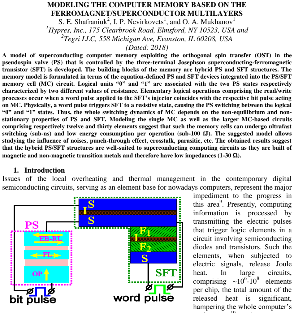
Introduction Issues of the local overheating and thermal management in the contemporary digital semiconducting circuits, serving as an element base for nowadays computers, represent the major impediment to the progress in this area 9. Presently, computing information is processed by transmitting the electric pulses that trigger logic elements in a circuit...
-
[2]
Therefore, the CAD tools serve to development the semiconducting integrated circuits
Modelling the PS and SFT devices Design, validating and optimizing the electronic circuits is accomplished using the computer aided design (CAD) and circuit simulations. Therefore, the CAD tools serve to development the semiconducting integrated circuits. However, the CAD tools are not well mature yet for working with the superconducting digital electroni...
-
[3]
SFT Josephson transistor To accomplish the switching between logical states of the two -terminal PS valve, we complement it with a three -terminal superconducting -ferromagnetic transistor (SFT) , whos e electrical circuit diagram is shown in Fig. A1 (in Appendix). Namely, the two devices, PS and SFT, are combined into a hybrid electronic circuit comprisi...
-
[4]
A1 and the respective SFT equation defined device (EDD) subcircuit is depicted in Fig
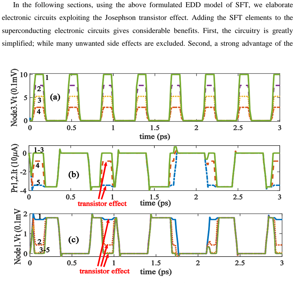
The electrical circuit diagram of SFT is shown in Fig. A1 and the respective SFT equation defined device (EDD) subcircuit is depicted in Fig. A2. Thus, when applying Eq. (1) to SFT, we assume that cI depends on the SFIFS injector bias current iI as shown in Fig. A2 (right). In our SFT circuits shown in Figs. A1, A2, the suppression of caI by the SFIFS inj...
-
[5]
The I -V curve is described by the RCSJ model (Resistively and Capacitively Shunted Junction) 17
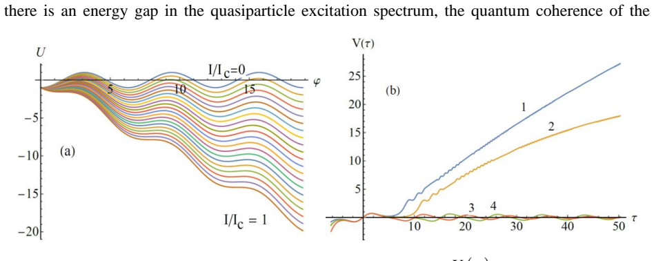
Hysteresis in the Josephson junctions The electric current I between two superconductors separated by a weak link forming a Josephson junction flows without dissipation until I reaches a critical current Ic, at which a finite bias voltage appears. The I -V curve is described by the RCSJ model (Resistively and Capacitively Shunted Junction) 17. In conventi...
-
[6]
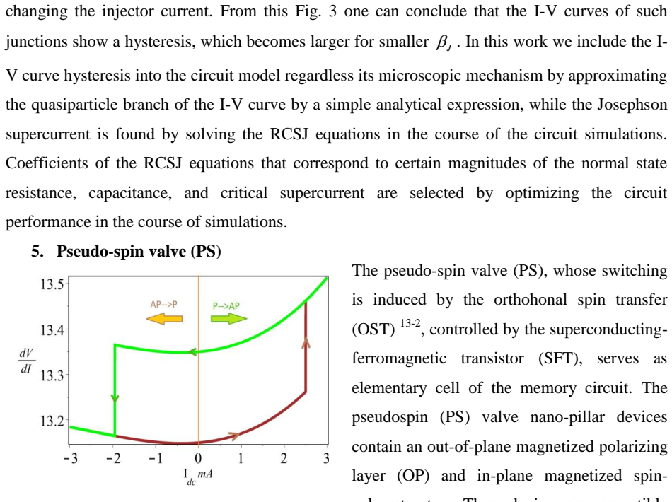
Pseudo-spin valve (PS) The pseudo-spin valve (PS), whose switching is induced by the orthohonal spin transfer (OST) 13-2, controlled by the superconducting- ferromagnetic transistor (SFT), serves as elementary cell of the memory circuit. The pseudospin (PS) valve nano -pillar devices contain an out-of-plane magnetized polarizing layer (OP) and in-plane ma...
-
[7]
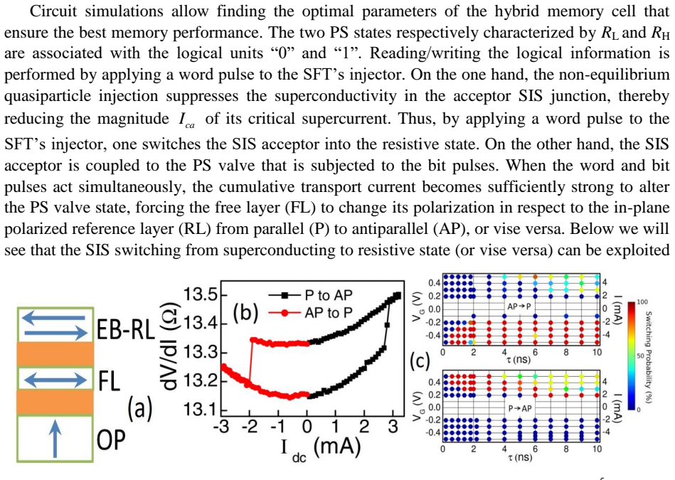
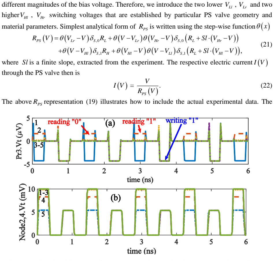
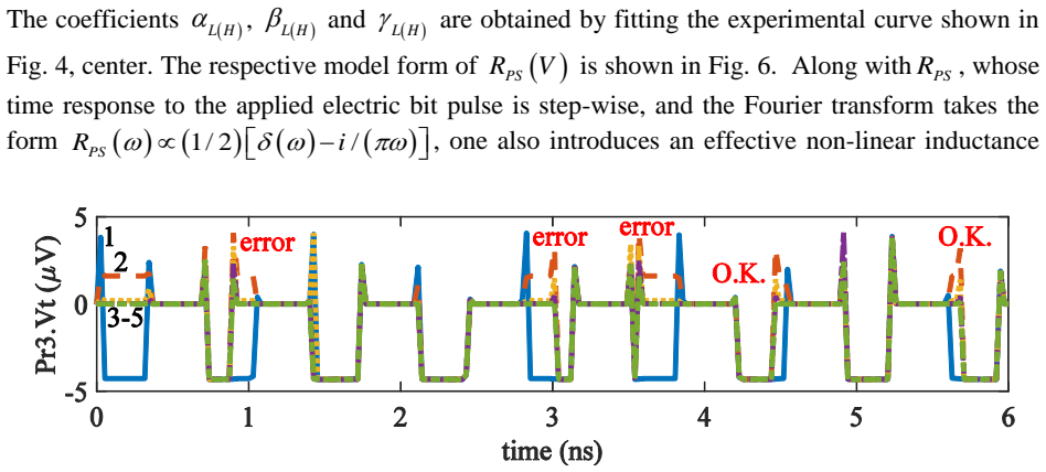
The PS/SFT memory cell Further in this work we elaborate the forth 01 and back 10 switching processes of the two-terminal PS characterized by two distinct magnitudes LR and HR of their resistance5-8, comprising respectively the two logical states “0” and “1”. We have developed model, describing switching dynamics of the PS valve, shown in Fig. 4. The PS...
-
[8]
0” “1” and negat ive pulses for the writing and reading “1
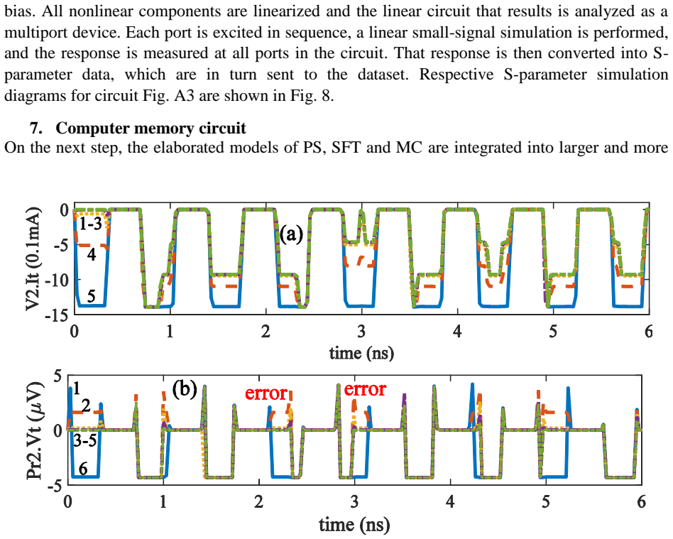
Computer memory circuit On the next step, the elaborated models of PS, SFT and MC are integrated into l arger and more complex superconducting computer memory circuits. In particular, we modeled the switching dynamics of the computer memory based on the orthogonal spin transfer (OST) involving the pseudospin valves (PS) and the multilayered superconductor...
-
[9]
0” “1” while the negative electrical pulses are implemented to writing/reading “1
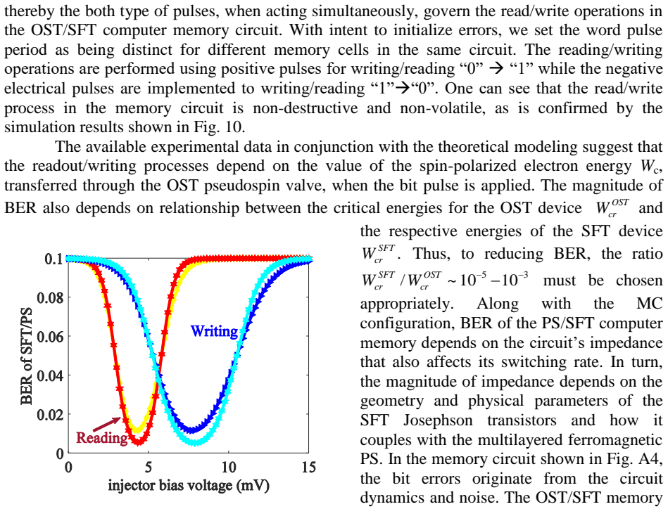
Read/write errors The origin of errors in the PS/SFT superconductor -ferromagnetic computer memory in the course of reading/writing the logical information has been examined as follows. We utilized the computer-aided design (CAD) of the experimental PS/SFT elements to studying the mechanisms of reading/writing errors in the PS/SFT memory. The errors were ...
-
[10]
Conclusions The above reported simulation results suggest that the hybrid computer memory is characterized by ultrafast switching (sub -ns) and low energy consumption per operation (sub -100 fJ) due to large initial spin -transfer torque from the perpendicular polarizer. Our model, describing the superconducting computer me mory circuits, also allows stud...
-
[11]
I. P. Nevirkovets, O. Chernyashevskyy, G. V. Prokopenko, O. A. Mukhanov and J. B. Ketterson, Control of Supercurrent in Hybrid Superconducting -Ferromagnetic Transistors. Ieee T Appl Supercon 25 (2015)
work page 2015
-
[12]
I. P. Nevirkoves, S. E. Shafraniuk, O. Chernyashevsk yy, D. T. Yohannes, O. Mukhanov and J. B. Kett erson, Critical Current Gain in High -j(c) Superconducting -Ferromagnetic Transistors. Ieee T Appl Supercon 26 (2016)
work page 2016
-
[13]
I. P. Nevirkovets, S. E. Shafraniuk, O. Chernyashevskyy, D. T. Yohannes, O. A. Mukhanov, J. B. Ketterson , Investigation of Current Gain in Superconducting-Ferromagnetic Transistors With High-j(c) Acceptor. Ieee T Appl Supercon 27 (2017)
work page 2017
-
[14]
Nevirkovets, I. P., Shafranjuk, S. E., Chernyashevskyy, O., Masilamani, N. & Ketterson, J. B. Current-voltage characteristics of Nb -carbon-Nb junctions. Low Temp Phys. 40, 191 -198 (2014)
work page 2014
-
[15]
L. Ye, D. B. Gopman, L. Rehm, D. Backes, G. Wolf, T. Ohki, A. F. Kirichenko, I. V. Vernik, O. A. Mukhanov, and A. D. Kent. Spin-transfer switching of orthogonal spin-valve devices at cryogenic temperatures. J Appl Phys 115 (2014)
work page 2014
-
[16]
Slonczewski, J. C. Current -driven excitation of magnetic multilayers. J Magn Magn Mater 159, L1-L7 (1996)
work page 1996
-
[17]
Emission of spin waves by a magnetic multilayer traversed by a current
Berger, L. Emission of spin waves by a magnetic multilayer traversed by a current. Phys Rev B 54, 9353-9358 (1996)
work page 1996
-
[18]
Ye, L., Wolf, G., Pinna, D., Chaves -O'Flynn, G. D. & Kent, A. D. State diagram of an orthogonal spin transfer spin valve device. J Appl Phys 117 (2015)
work page 2015
-
[19]
Mukhanov, O. A. Energy -Efficient Single Flux Quantum Technology. Ieee T Appl Supercon 21, 760-769 (2011)
work page 2011
-
[20]
S. V. Bakurskiy, V. I. Filippov, V. I. Ruzhickiy, N. V. Klenov, I. I. Soloviev, M. Yu. Kupriyanov, and A. A. Golubov , Current-phase relations in SIsFS junctions in the vicinity of 0-pi transition. Phys Rev B 95 (2017)
work page 2017
-
[21]
Kornev, V. K., Soloviev, I. I., Klenov, N. V., Sharafiev, A. V. & Mukhanov, O. A. Linear Bi-SQUID Arrays for Electrically Small Antennas. Ieee T Appl Supercon 21, 713-716 (2011)
work page 2011
-
[22]
Mukhanov, O. A., Kirichenko, A. F., Filippov, T. V. & Sarwana, S. Hybrid Semiconductor-Superconductor Fast-Readout Memory for Digital RF Receivers. Ieee T Appl Supercon 21, 797-800 (2011)
work page 2011
-
[23]
Holmes, D. S., Kadin, A. M. & Johnson, M. W. Superconducting Computing in Large - Scale Hybrid Systems. Computer 48, 34-42 (2015)
work page 2015
-
[24]
Likharev, K. K. Dynamics of Josephson Junctions and Circuits. 1 edn, (CRC Press, 1986)
work page 1986
-
[25]
Thermoelectricity and Heat Transport in Graphene and Other 2D Nanomaterials
Shafraniuk, S. Thermoelectricity and Heat Transport in Graphene and Other 2D Nanomaterials. (Elsevier - Health Sciences Division, 2017)
work page 2017
-
[26]
Likharev, K. K. Superconductor digital electronics. Physica C -Superconductivity and Its Applications 482, 6-18 (2012)
work page 2012
-
[27]
Likharev, K. K. & Semenov, V. K. RSFQ Logic/Memory Family: A New Josephson - Junction Technology for Sub -Terahertz-Clock-Frequency Digital Systems. Ieee T Appl Supercon 1, 3-28 (1991)
work page 1991
-
[28]
Shafranjuk, S., Nevirkovets, I. P., Mukhanov, O. A. & Ket terson, J. B. Control of Superconductivity in a Hybrid Superconducting/Ferromagnetic Multilayer Using Nonequilibrium Tunneling Injection. Phys Rev Appl 6 (2016)
work page 2016
-
[29]
K. Gaj, Q. Herr, V. Adler, A. Krasniewski, E. G. Friedman, M. S. Feldman , Tools for the computer-aided design of multigigahertz superconducting digital circuits. Ieee T Appl Supercon 9, 18-38 (1999)
work page 1999
-
[30]
Kalinov, A. V., Voloshin, I. F. & Fisher, L. M. SPICE model of high -temperature superconducting tape: application to resistive fault -current limiter. Supercond Sci Tech 30 (2017)
work page 2017
-
[31]
Shen, B., Jiang, J. F. & Cai, Q. Y. Simulation of circuits composed of HTSC -single hole transistors by using superconducting SET-SPICE. Physica C 341, 1605-1606 (2000)
work page 2000
-
[32]
Hernandez, S. & Victora, R. H. Calculation of spin transf er torque in partially polarized spin valves including multiple reflections. Appl Phys Lett 97 (2010)
work page 2010
-
[33]
Qiu, Y. C., Zhang, Z. Z., Jin, Q. Y. & Liu, Y. W. Dynamic dipolar interaction effect on spin-transfer switching with perpendicular anisotropy. Appl Phys Lett 95 (2009)
work page 2009
-
[34]
Zhu, X. C. & Kang, S. H. Inherent spin transfer torque driven switching current fluctuations in magnetic element with in -plane magnetization and comparison to perpendicular design. J Appl Phys 106 (2009)
work page 2009
-
[35]
Lee, K., Chen, W. C., Zhu, X. C., L i, X. & Kang, S. H. Effect of interlayer coupling in CoFeB/Ta/NiFe free layers on the critical switching current of MgO -based magnetic tunnel junctions. J Appl Phys 106 (2009)
work page 2009
-
[36]
Zhu, X. C. & Kang, S. H. Distinction and correlation between magnetization swit chings driven by spin transfer torque and applied magnetic field. J Appl Phys 105 (2009)
work page 2009
-
[37]
Carpentieri, M., Torres, L. & Martinez, E. Micromagnetic study of spin -transfer driven ferromagnetic resonance: Equivalent circuit. J Appl Phys 106 (2009)
work page 2009
-
[38]
Carpentieri, M., Torres, L. & Martinez, E. Temperature Dependence of Microwave Nano-Oscillator Linewidths Driven by Spin -Polarized Currents: A Micromagnetic Analysis. Ieee T Magn 45, 3426-3429 (2009)
work page 2009
-
[39]
Carpentieri, M., Torres, L. & Martinez, E. Effective Damping Cont ribution From Micromagnetic Modeling in a Spin -Transfer-Driven Ferromagnetic Resonance. Ieee T Nanotechnol 8, 477-481 (2009)
work page 2009
-
[40]
B. Baek, W. H. Rippard, S. P. Benz, S. E. Russek, & P. D. Dresselhaus, Hybrid superconducting-magnetic memory device using competing order parameters. Nat Commun 5 (2014)
work page 2014
-
[41]
B. Baek, W. H. Rippard, M. R. Pufall, S. P. Benz, S. E. Russek, H. Rogalla, P. D. Dresselhaus, Spin-Transfer Torque Switching in Nanopillar Superconducting -Magnetic Hybrid Josephson Junctions. Phys Rev Appl 3 (2015)
work page 2015
-
[42]
C. Bell, G. Burnell, C. W. Leung, E. J. Tarte, D. -J. Kang, and M. G. Blamire , Controllable Josephson current through a pseudospin -valve structure. Appl Phys Lett 84, 1153-1155 (2004)
work page 2004
-
[43]
M. A. El Qader, R. K. Singh, S. N. Galvin, L. Yu, J. M. Rowell, and N . Newman , Switching at small magnetic fields in Josephson junctions fabricated with ferromagnetic barrier layers, Appl. Phys. Lett. 104, 022602 (2014)
work page 2014
-
[44]
Jain, A., Ghosh, A., Singh, N. B. & Sarkar, S. K. A new SPICE macro model of single electron transistor for efficient simulation of single -electronics circuits. Analog Integr Circ S 82, 653-662 (2015)
work page 2015
-
[45]
W. Grabinski, M. Brinson, P. Nenzi, F. Lannutti, N. Makris, A. Antonopoulos, M. Bucher, Open-source circuit simulation tools for RF compact semiconductor device modelling. Int J Numer Model El 27, 761-779 (2014)
work page 2014
-
[46]
Brinson, M. E. & Kuznetsov, V. A new approach to compact semiconductor device modelling with Qucs Verilog -A analogue module synthesis. Int J Numer Model El 29, 1070 - 1088 (2016)
work page 2016
-
[47]
Brinson, M. E. & Nabijou, H. Adaptive subcircuits and compact Verilog -A macromodels as integrated design and analysis blocks in Qucs circuit simulation. Int J Electron 98, 631 -645 (2011)
work page 2011
-
[48]
Brinson, M. E. & Jahn, S. Qucs: A GPL software package for circuit simulation, compact device modelling and circuit macromodelling from DC to RF and beyond. Int J Numer Model El 22, 297-319 (2009)
work page 2009
-
[49]
Jahn, S. & Brinson, M. E. Interactive compact device modelling using Qucs equation - defined devices. Int J Numer Model El 21, 335-349 (2008)
work page 2008
-
[50]
Energy Gap in Superconductors Measured by Electron Tunneling
Giaever, I. Energy Gap in Superconductors Measured by Electron Tunneling. Phys Rev Lett 5, 147-148 (1960)
work page 1960
-
[51]
Pinna, D., Stein, D. L. & Kent, A. D. Spin -torque oscillators with thermal noise: A constant energy orbit approach. Phys Rev B 90 (2014)
work page 2014
-
[52]
Pinna, D., Kent, A. D. & Stein, D. L. Thermally assisted spin -transfer torque dynamics in energy space. Phys Rev B 88 (2013)
work page 2013
-
[53]
Courtois, H., Meschke, M., Peltonen, J. T. & Pekola, J. P. Origin of hysteresis in a proximity Josephson junction. Phys Rev Lett 101 (2008)
work page 2008
-
[54]
Rogovin, D. & Scalapino, D. J. Fluctuation Phenomena in Tunnel -Junctions. Ann Phys - New York 86, 1-90 (1974). Fig. 5A1. Test circuit of SFT serving as the Josephson transistor 1-4, whose geometry is shown on the left (reproduced with permissions from APS, Ref. 18) . We perform dc simulations, Harmonic balance simulations, ac simulations, and transient ...
work page 1974
-
[55]
N. Ruppelt, H. Sickinger, R. Menditto, E. Goldobin, D. Koelle, R. Kleiner, O. Vavra, and H. Kohlsted, Observation of 0 –p transition in SIsFS Josephson junctions, Applied Physics Letters 106, 022602 (2015)
work page 2015
-
[56]
A. Moor, A. F. Volkov, and K. B. Efetov, Inhomogeneous state in nonequilibrium superconductor/normal-metal tunnel structures: A Larkin -Ovchinnikov-Fulde-Ferrell-like phase for nonmagnetic systems, Phys. Rev. B 80, 054516 (2009)
work page 2009
-
[57]
J. J. A. Baselmans, A. F. Morpurgo, B. J. van Wees & T. M. Klapwijk, Reversing the direction of the supercurrent in a controllable Josephson junction, Nature 397, 43–45 (1999)
work page 1999
-
[58]
Appendix A1. The test circuit of SFT Fig. A1 shows the geometry (left panel) and the electrical circuit diagram (right panel) of the three-terminal superconducting -ferromagnetic transistor (SFT). Mathematical details of the model are given in Sec. 3 of the main text. A2. Respective subcircuit to the SFT equation defined device (EDD) Fig. A2. Left: Subcir...
discussion (0)
Sign in with ORCID, Apple, or X to comment. Anyone can read and Pith papers without signing in.