REVIEW 3 major objections 5 minor 66 references
Simulation of single hole spin qubit in strained triangular FinFET quantum devices
T0 review · 3 major / 5 minor · reviewed 2026-08-07 · deepseek-v4-flash
Pith's one-line read Cooling a silicon FinFET to cryogenic temperatures strains its channel, and the sign of that strain, set by which parts of the device are held fixed, determines which hole states form the qubit ground state.
desk verdict A solid simulation study showing cooling-induced strain matters for FinFET hole spin qubits; the qualitative message is convincing, but the specific claim that compressive strain is the real scenario is underdetermined by one Rabi-frequency match. read the letter →
The pith
A machine-rendered reading of the paper's core claim, the machinery that carries it, and where it could break.
The reading
What carries the argument
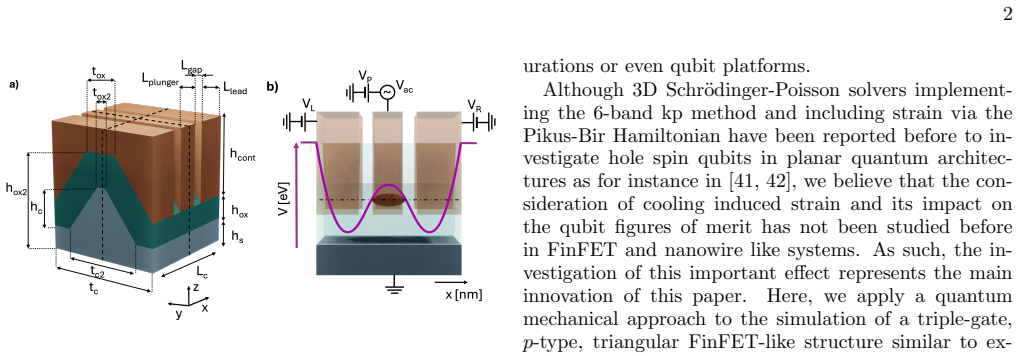
The argument runs on three coupled pieces of machinery. First, a self-consistent Schrödinger-Poisson solver built on the 6×6 Luttinger-Kohn $k\cdot p$ Hamiltonian on a finite-difference grid, which resolves the triangular channel's nontrivial confinement and captures heavy-hole, light-hole, and split-off band mixing; strain enters through the Pikus-Bir deformation potentials acting on the strain tensor components. Second, a finite-element thermo-mechanical model of the cooling contraction of the Si/SiO2/TiN stack, whose outcome is controlled entirely by two boundary-condition scenarios: BC1 (only the substrate fixed) yields compression in the channel, while BC2 (gate outer faces also fixed) yields tension. Third, a g-matrix formalism that reconstructs the full g-tensor from energy splittings under magnetic fields along six independent directions and computes Rabi frequencies from the derivative of the g-matrix with respect to the plunger-gate voltage, linking the strain-modified wave functions to measurable qubit figures of merit.
What would settle it
Measure the actual strain state inside the silicon channel of a comparable FinFET at cryogenic temperature, or measure the Rabi frequency of the same device at several magnetic-field orientations: if the channel is found to be under tension (positive $\varepsilon_{zz}$), or if the measured Rabi map matches the BC2 prediction rather than the BC1 prediction, the paper's central conclusion that cooling produces compressive strain collapses.
Extended reading notes
Core claim
The central claim is that thermally induced strain, produced when a FinFET cools from 300 K to 4 K, substantially renormalizes the hole spin qubit ground state, and that the nature of the strain is set by the thermo-mechanical boundary conditions. In the authors' 6×6 Luttinger-Kohn $k\cdot p$ simulations with Pikus-Bir strain terms, compressive strain (BC1, substrate fixed) shifts the ground state toward light-hole character, while tensile strain (BC2, gate outer faces anchored as well) keeps heavy-hole character and strongly increases the ground-to-excited-state splitting (from 0.8 to 5.6 meV in one geometry) and the Rabi frequency (8.5 MHz versus 104 MHz). The g-tensor loses anisotropy under both strain scenarios. When the computed metrics are compared with a measured triangular FinFET hole qubit, the unstrained simulation fails qualitatively, while the compressed-channel scenario reproduces the measured Rabi frequency (8.5 vs 10 MHz), the energy splitting (2.6 vs 3.3 meV), and g-factor magnitudes in the right range. The paper therefore concludes that cooling-induced compression is the likely strain state in these devices and that strain inclusion is indispensable for modeling hole spin qubits.
Load-bearing premise
The load-bearing assumption is that the real cooling deformation is bracketed by the two chosen boundary-condition scenarios and described by linear, temperature-invariant thermal expansion: if the actual strain in the silicon channel differs in sign, magnitude, or spatial pattern, for example through residual fabrication strain, every computed qubit metric and the conclusion that compression is realistic would be unreliable.
Editorial extensions
If this is right
- Unstrained simulations of hole spin qubits in FinFETs miss the dominant physics: in this device the ground-to-excited-state splitting rises from 0.8 meV to 2.6–2.7 meV only when cooling strain is included.
- The sign of the cooling strain, not the channel geometry, dictates the ground-state band character: compression favors light holes, tension favors heavy holes, across all three fin cross-sections studied.
- The realistic cooling scenario for a FinFET with a fixed substrate and a freely contracting stack is compression, as judged by matching the measured Rabi frequency (8.5 MHz computed vs 10 MHz measured) and energy splitting of a comparable device.
- Tensile strain, if it could be engineered by anchoring the gates, would produce faster qubit driving (multiplying the Rabi frequency by more than ten in this geometry) at the price of altering the g-tensor anisotropy.
- Crystallographic orientation and magnetic-field angle interact with the strain to create structured Rabi-frequency maps, giving design choices for maximizing driving strength.
Reading between the lines
- The paper's verdict that compression is realistic rests on matching one scalar, the Rabi frequency at a single magnetic-field orientation; a stronger test would compare the full computed and measured Rabi maps over magnetic-field angles, since the two scenarios differ dramatically there.
- Strain also changes the spatial distribution of the spin-orbit basis states, so dephasing from charge noise, which is not computed here, should shift with strain; the 'sweet spots' identified in earlier FinFET qubit studies may move or disappear under realistic cooling strain.
- Direct strain metrology in the channel, for instance X-ray or Raman measurements on a cooled device, would settle the BC1-versus-BC2 ambiguity and could calibrate the thermo-mechanical model parameters.
- The same solver platform could be applied to planar or nanowire hole qubits, where the strain distribution from a known substrate and gate stack is more constrained and the two boundary-condition scenarios could be discriminated.
Editorial analysis
A structured set of objections, weighed in public.
Referee Report
Summary. The paper presents simulation of a single hole spin qubit in a triple-gate triangular Si FinFET, using an in-house self-consistent Schrödinger-Poisson solver with a 6-band Luttinger-Kohn k.p Hamiltonian. It adds thermally induced strain via linear thermo-elastic finite-element calculations, considering two boundary-condition scenarios: BC1 (fixed substrate only, leading to compressive channel strain) and BC2 (fixed substrate and gate outer faces, leading to tensile strain). The paper computes dot length, band mixing, g-tensor, and Rabi frequency under no strain, BC1, and BC2, and compares the results with experimental data from Camenzind et al. (Ref. [37]). The central claims are that cooling-induced strain strongly renormalizes the qubit metrics and that the compressive scenario BC1 is more likely to occur, based on the simulated Rabi frequency of 8.5 MHz being close to the measured 10 MHz while BC2 gives 104 MHz.
Significance. The qualitative finding that cooling-induced strain substantially modifies the hole qubit ground state, band mixing, g-factors, and Rabi frequencies is significant for the modeling and design of silicon FinFET hole spin qubits. The paper's methodology is sound within the 6-band k.p framework: no parameters are fitted to the experimental target metrics, and the g-factors and Rabi frequencies are computed from the Hamiltonian using literature material parameters, with open data provided (Zenodo, Ref. [60]). The comparison with experiment also demonstrates that including strain is necessary to bring the computed energy splitting and g-factors closer to measured values. However, the specific conclusion that compression (BC1) is more realistic than tension (BC2) rests on a single experimental Rabi frequency and is not yet load-bearing. The robust and useful claim is that thermal contraction strain must be included and that its sign and magnitude can strongly alter qubit figures of merit; the discrimination between the two scenarios requires stronger experimental and modeling support.
major comments (3)
- [§III.D and Eq. (11)] The conclusion that BC1 (compressive strain) is more realistic than BC2 (tensile strain) rests entirely on matching one experimental Rabi frequency: the simulated 8.5 MHz (BC1) and 104 MHz (BC2) are compared with the measured 10 MHz for Q2 in Ref. [37] (Table II). This single-number comparison is not yet a reliable discriminator because the Rabi frequency calculation depends on several unsupported modeling choices, including the temperature-independent thermal expansion coefficient α in Eq. (11) multiplied by (T_cool - T_rt), the two fictitious boundary-condition scenarios, and the scaled single-dot geometry. The paper itself notes that there is "a priori no straightforward way to precisely extract the strain distribution inside the silicon channel" (Section II.C) and that residual fabrication strain is neglected. The qualitative statement that strain renormalizes qubit metrics is well supported, but the more-likely-compression conclusion requires additional justification or should be reframed as tentative.
- [§II.C and §III.D] The two boundary-condition scenarios BC1 and BC2 are presented without uncertainty quantification or sensitivity analysis. The strain tensor components entering the Pikus-Bir terms in Eq. (12) differ in sign and magnitude between the scenarios (e.g., ε_zz ≈ -2.5×10^-3 for BC1 versus +3×10^-3 for BC2, Section III.A), and the measured metrics in Table II do not clearly favor one scenario: the g-factors and energy splitting ∆ are in "relatively good agreement" with experiment for both BC1 and BC2. Only the Rabi frequency separates them. Because the sign of the strain depends on the assumed boundary conditions, and because the real device could have an intermediate or inhomogeneous strain field, the conclusion that the compression scenario is more likely cannot be drawn from the current evidence. A sensitivity study varying α, the cooling temperature integral, and the boundary conditions, or a direct strain measurement, would be needed.
- [§III.D and Eq. (5)] The comparison with experiment is performed in a scaled, single-dot version of the experimental double-dot device, with the barrier gate and second dot absent. The paper acknowledges that the additional gate "induces an additional electrostatic confinement inside the channel that is not considered in our simulations, but could increase both the energy spacing ∆ and the g-factor g_x" (end of Section III.D). Since the BC1-versus-BC2 discrimination relies on the Rabi frequency, which is sensitive to the dot shape and g-tensor derivative, this geometric simplification weakens the central comparison. In addition, the Rabi frequency from Eq. (5) uses g-matrix derivatives obtained at V0 ± δV, but no convergence check with respect to δV is reported; the robustness of the 8.5 MHz versus 104 MHz difference to this numerical parameter is not established.
minor comments (5)
- [§II.A] There is a typo in the sentence "the device was extended on boths side with two, 2-nm-thick and highly p-doped regions": "boths side" should be "both sides".
- [Fig. 5 caption] The caption contains the typo "from Geo1 to Goe3"; "Goe3" should be "Geo3".
- [§III.B and Fig. 6] The geometry labels are inconsistent: the text uses "Geo1", "Geo2", and "Geo3", but in the discussion of Fig. 6 the symbol "Ge3" appears once; please unify the notation.
- [References] Reference [53] appears incomplete, as the journal name is missing from the citation; please complete the bibliographic information.
- [§III.A and Fig. 4] In the text, the qubit location is described as enclosed by "gray dotted trapezoids" in Fig. 4, while earlier the same enclosure is called "gray dashed trapezoids" in Fig. 3; please make the descriptions consistent.
Circularity Check
No significant circularity: the simulations are self-contained, experimental data are used only as a post-hoc benchmark, and the BC1/BC2 scenarios are modeling assumptions rather than fitted parameters.
full rationale
The paper's central result is that cooling-induced strain renormalizes the hole spin qubit metrics. This is derived from a first-principles-style chain: the 6x6 Luttinger-Kohn k.p Hamiltonian with literature material parameters, the Pikus-Bir strain Hamiltonian of Eqs. (12a)-(12d), and a finite-element thermo-mechanical calculation using Eq. (10)-(11). No parameter is fitted to the experimental targets (g-factors, Rabi frequency, dot length, or splitting). The experimental values from Ref. [37] appear only in Table II as a comparison after the fact, not as inputs to the simulation. The two boundary-condition scenarios, BC1 and BC2, are explicitly introduced as alternative modeling assumptions ('fictitious, yet realistic cooling scenarios'), and neither is calibrated to reproduce the measured Rabi frequency. The statement that the compressive scenario (BC1) is 'more likely' is an inference from the closer agreement of one computed Rabi frequency (8.5 MHz vs 104 MHz) with the measured 10 MHz; this is model selection based on an external benchmark, not a fitted parameter renamed as a prediction. The Pikus-Bir argument that negative epsilon_zz favors LH character is derived directly from Eqs. (12a)-(12b) and the sign of the strain, not from the experimental outcomes. Self-citations are limited to the in-house solver methodology ([43]) and the data repository ([60]), neither of which is load-bearing for the physics claims. The acknowledged uncertainties in the strain model, including the linear temperature-invariant alpha in Eq. (11) and the absence of residual fabrication strain, are correctness risks rather than circularity. Therefore the derivation chain does not reduce to its own inputs.
Assumptions & free parameters
free parameters (2)
- Operating gate voltages (V_L,R, V_P) =
V_L,R = 0.78 V, V_P = 0.38 V for Geo1; 0.84 V and 0.33 V for Geo2; 0.84 V and 0.36 V for Geo3; 0.82 V and 0.40 V for…
- Effective mass m* for experimental dot length conversion =
0.45 m_e
assumptions (5)
- domain assumption The 6-band Luttinger-Kohn k.p Hamiltonian with Pikus-Bir strain terms accurately describes hole spin qubit ground states in Si FinFETs.
- domain assumption Linear elastic, temperature-invariant thermal contraction with no residual strain represents the cooling process.
- ad hoc to paper The two boundary condition scenarios BC1 and BC2 bracket the real mechanical constraints of the device.
- standard math The g-matrix formalism and Rabi frequency formula from Ref. [47] apply to this device.
- domain assumption Hard-wall boundary conditions and no wavefunction penetration into oxide or substrate are valid.
Cite this review
Pith. "Pith review of Simulation of single hole spin qubit in strained triangular FinFET quantum devices." pith.science (2026). https://pith.science/paper/KJU3IEGK
@misc{pith2026250522267,
  author       = {Pith},
  title        = {Pith review of: Simulation of single hole spin qubit in strained triangular FinFET quantum devices},
  year         = {2026},
  howpublished = {\url{https://pith.science/paper/KJU3IEGK}},
  note         = {Machine review of arXiv:2505.22267}
}
read the original abstract
Using an in-house Schroedinger-Poisson (SP) solver, we investigate the creation of a single hole spin qubit inside a triple-gate triangular silicon fin field effect transistor (Si FinFET) quantum device similar to experimental structures. The gate induced formation of the required quantum dot (QD) is monitored based on the Luttinger-Kohn 6x6 kp method accounting for magnetic fields and strain to determine the qubit ground state. Strain arises from the inhomogeneous contraction of the different FinFET components when they are cooled down to cryogenic temperatures. It leads to a renormalization of the qubit energy levels, thus impacting both the heavy-hole (HH) and light-hole (LH) populations as well as their mixing. The dot length, band mixing, g-factor, and Larmor/Rabi frequencies of the considered device are extracted. In particular, we show that these metrics exhibit strong strain-dependent variations of their magnitude, thus underlying the importance of including realistic thermal contraction scenarios when modeling hole spin qubits.
Figures


Figures from the paper (11 more)




Reference graph
Works this paper leans on
-
[37]
191 (Springer, Berlin Heidelberg, 2003)
Roland Winkler,Spin-orbit coupling effects in two- dimensional electron and hole systems: with 26 tables, Springer tracts in modern physics Solid-state physics No. 191 (Springer, Berlin Heidelberg, 2003)
work page 2003
-
[60]
Simulation output data of triangu- lar quantum finfet device,
Ilan Bouquet, “Simulation output data of triangu- lar quantum finfet device,” (2025), 10.5281/zen- odo.15224899
doi:10.5281/zen- 2025
-
[1]
Analytical expressions from the Peierls substitution With the magnetic fieldB=(B x,By,Bz), the gauge: A=−(B zy,0, Byx−B xy), andB=∇×Awe obtain for the different components ofk ˜kx =k x − e ℏ Bzy(A2) ˜ky =k y (A3) ˜kz =k z − e ℏ (Byx−B xy).(A4) We then rewrite thek ikj terms present in the Hamil- tonian as 1 2 (kikj +k jki) and setk ij∝∂ i(j) = 0 for i, j=...
-
[2]
Discretized form of the vector potential contributions We perform the two-step substitution: kα → −i∂α forα=x, y, zand β∂αΨ = Ψi+1 −Ψ i−1 2∆α βi where Ψ is the wave function vector. Accounting now only for the non-diagonal terms and settingT 1 =e/ℏto we have ˜k2 x :i T1Bzyijk ∆x (Ψi+1jk −Ψ i−1jk )∝L, M(A11) ˜k2 z :i T1 ∆z (Byxijk −B xyijk )(Ψijk+1 −Ψ ijk−...
-
[3]
Calculation on the magnetic operator for the g-matrix creation Following the notation given in [47], we can calcu- late the matrix elements ofM 1 using the finite difference method. For instance ⟨ψ1|M1,y|ψ2⟩=− 1 2δB [⟨ψ1|H(V,+δBy)|ψ 2⟩ − ⟨ψ1|H(V,−δBy)|ψ 2⟩] (A19) , where the 6×6 diagonal blocks ofHare given by Eq. 2 and the off-diagonal ones by Eq. A16-A1...
-
[4]
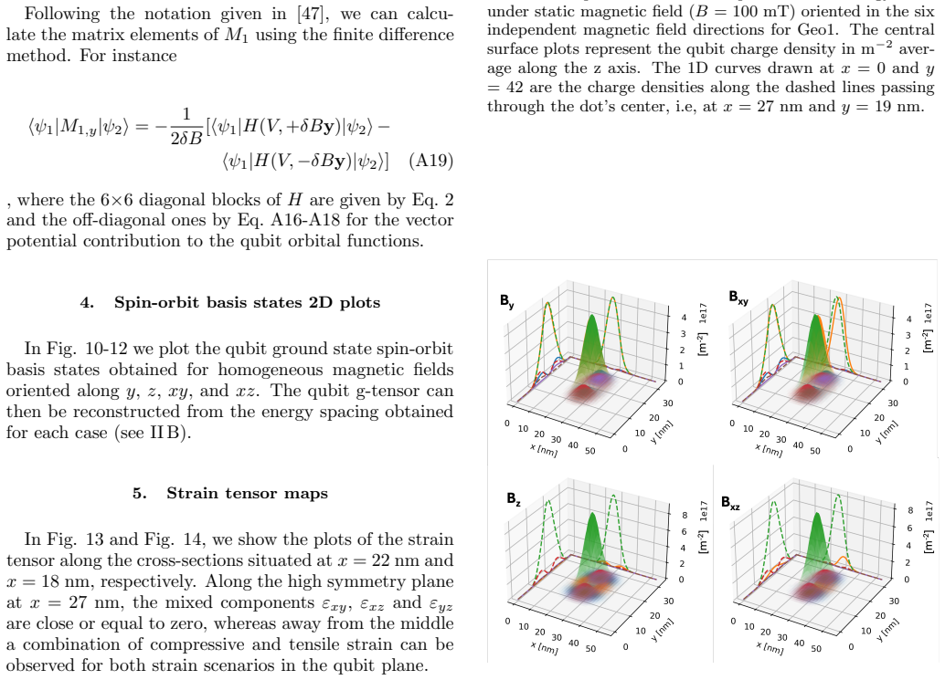
Spin-orbit basis states 2D plots In Fig. 10-12 we plot the qubit ground state spin-orbit basis states obtained for homogeneous magnetic fields oriented alongy,z,xy, andxz. The qubit g-tensor can then be reconstructed from the energy spacing obtained for each case (see II B)
-
[5]
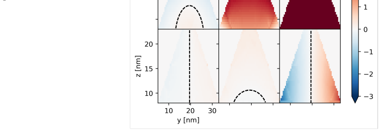
Strain tensor maps In Fig. 13 and Fig. 14, we show the plots of the strain tensor along the cross-sections situated atx= 22 nm and x= 18 nm, respectively. Along the high symmetry plane atx= 27 nm, the mixed componentsε xy,ε xz andε yz are close or equal to zero, whereas away from the middle a combination of compressive and tensile strain can be observed f...
-
[6]
Semiconductor spin qubits,
Guido Burkard, Thaddeus D. Ladd, Andrew Pan, John M. Nichol, and Jason R. Petta, “Semiconductor spin qubits,” Rev. Mod. Phys.95, 025003 (2023)
2023
Show all 66 references
-
[7]
Quantum com- putation with quantum dots,
Daniel Loss and David P. DiVincenzo, “Quantum com- putation with quantum dots,” Phys. Rev. A57, 120–126 (1998)
1998
-
[8]
Coupled quantum dots as quantum gates,
Guido Burkard, Daniel Loss, and David P. DiVincenzo, “Coupled quantum dots as quantum gates,” Phys. Rev. B59, 2070–2078 (1999)
1999
-
[9]
Prospects for Spin- Based Quantum Computing,
Christoph Kloeffel and Daniel Loss, “Prospects for Spin- Based Quantum Computing,” Annu. Rev. Condens. Mat- ter Phys.4, 51–81 (2013), arXiv:1204.5917 [cond-mat]
2013 arXiv
-
[10]
Spins in few-electron quan- tum dots,
R. Hanson, L. P. Kouwenhoven, J. R. Petta, S. Tarucha, and L. M. K. Vandersypen, “Spins in few-electron quan- tum dots,” Rev. Mod. Phys.79, 1217–1265 (2007)
2007
-
[11]
Silicon quantum electronics,
Floris A. Zwanenburg, Andrew S. Dzurak, Andrea Morello, Michelle Y. Simmons, Lloyd C. L. Hollenberg, Gerhard Klimeck, Sven Rogge, Susan N. Coppersmith, and Mark A. Eriksson, “Silicon quantum electronics,” Rev. Mod. Phys.85, 961–1019 (2013)
2013
-
[12]
Fidelity benchmarks for two-qubit gates in silicon,
W. Huang, C. H. Yang, K. W. Chan, T. Tanttu, B. Hensen, R. C. C. Leon, M. A. Fogarty, J. C. C. Hwang, F. E. Hudson, K. M. Itoh, A. Morello, A. Laucht, and A. S. Dzurak, “Fidelity benchmarks for two-qubit gates in silicon,” Nature569, 532–536 (2019)
2019
-
[13]
Electrical control of a long-lived spin qubit in a Si/SiGe quantum dot,
E. Kawakami, P. Scarlino, D. R. Ward, F. R. Braakman, D. E. Savage, M. G. Lagally, Mark Friesen, S. N. Cop- persmith, M. A. Eriksson, and L. M. K. Vandersypen, “Electrical control of a long-lived spin qubit in a Si/SiGe quantum dot,” Nature Nanotech9, 666–670 (2014)
2014
-
[14]
A fault-tolerant addressable spin qubit in a natural silicon quantum dot,
Kenta Takeda, Jun Kamioka, Tomohiro Otsuka, Jun Yoneda, Takashi Nakajima, Matthieu R. Delbecq, Shinichi Amaha, Giles Allison, Tetsuo Kodera, Shunri Oda, and Seigo Tarucha, “A fault-tolerant addressable spin qubit in a natural silicon quantum dot,” Sci. Adv. 2, e1600694 (2016)
2016
-
[15]
Resonantly driven CNOT gate for electron spins,
D. M. Zajac, A. J. Sigillito, M. Russ, F. Borjans, J. M. Taylor, G. Burkard, and J. R. Petta, “Resonantly driven CNOT gate for electron spins,” Science359, 439–442 (2018)
2018
-
[16]
A programmable two- qubit quantum processor in silicon,
T. F. Watson, S. G. J. Philips, E. Kawakami, D. R. Ward, P. Scarlino, M. Veldhorst, D. E. Savage, M. G. Lagally, Mark Friesen, S. N. Coppersmith, M. A. Eriks- son, and L. M. K. Vandersypen, “A programmable two- qubit quantum processor in silicon,” Nature555, 633– 637 (2018)
2018
-
[17]
A two-qubit logic gate in silicon,
M. Veldhorst, C. H. Yang, J. C. C. Hwang, W. Huang, J. P. Dehollain, J. T. Muhonen, S. Simmons, A. Laucht, F. E. Hudson, K. M. Itoh, A. Morello, and A. S. Dzurak, “A two-qubit logic gate in silicon,” Nature526, 410–414 (2015)
2015
-
[18]
Shallow and Undoped Germanium Quantum Wells: A Playground for Spin and Hybrid Quantum Technology,
Amir Sammak, Diego Sabbagh, Nico W. Hendrickx, Mario Lodari, Brian Paquelet Wuetz, Alberto Tosato, LaReine Yeoh, Monica Bollani, Michele Virgilio, Markus Andreas Schubert, Peter Zaumseil, Giovanni Capellini, Menno Veldhorst, and Giordano Scappucci, “Shallow and Undoped Germani...
2019
-
[19]
Universal quantum logic in hot silicon qubits,
L. Petit, H. G. J. Eenink, M. Russ, W. I. L. Lawrie, N. W. Hendrickx, S. G. J. Philips, J. S. Clarke, L. M. K. Vandersypen, and M. Veldhorst, “Universal quantum logic in hot silicon qubits,” Nature580, 355–359 (2020)
2020
-
[20]
Oper- ation of a silicon quantum processor unit cell above one kelvin,
C. H. Yang, R. C. C. Leon, J. C. C. Hwang, A. Saraiva, T. Tanttu, W. Huang, J. Camirand Lemyre, K. W. Chan, K. Y. Tan, F. E. Hudson, K. M. Itoh, A. Morello, M. Pioro-Ladri` ere, A. Laucht, and A. S. Dzurak, “Oper- ation of a silicon quantum processor unit cell above one kelvin...
2020
-
[21]
Fast universal quantum gate above the fault-tolerance threshold in silicon,
Akito Noiri, Kenta Takeda, Takashi Nakajima, Takashi Kobayashi, Amir Sammak, Giordano Scappucci, and Seigo Tarucha, “Fast universal quantum gate above the fault-tolerance threshold in silicon,” Nature601, 338–342 (2022)
2022
-
[22]
High-Fidelity State Prepara- tion, Quantum Control, and Readout of an Isotopically Enriched Silicon Spin Qubit,
A.R. Mills, C.R. Guinn, M.M. Feldman, A.J. Sigillito, M.J. Gullans, M.T. Rakher, J. Kerckhoff, C.A.C. Jack- son, and J.R. Petta, “High-Fidelity State Prepara- tion, Quantum Control, and Readout of an Isotopically Enriched Silicon Spin Qubit,” Phys. Rev. Applied18, 064028 (2022)
2022
-
[23]
The germanium quantum informa- tion route,
Giordano Scappucci, Christoph Kloeffel, Floris A. Zwa- nenburg, Daniel Loss, Maksym Myronov, Jian-Jun Zhang, Silvano De Franceschi, Georgios Katsaros, and Menno Veldhorst, “The germanium quantum informa- tion route,” Nat Rev Mater6, 926–943 (2020)
2020
-
[24]
Direct Rashba spin-orbit interaction in Si and Ge nanowires with different growth directions,
Christoph Kloeffel, Marko J. Ranˇ ci´ c, and Daniel Loss, “Direct Rashba spin-orbit interaction in Si and Ge nanowires with different growth directions,” Phys. Rev. B97, 235422 (2018)
2018
-
[25]
A single-hole spin qubit,
N. W. Hendrickx, W. I. L. Lawrie, L. Petit, A. Sam- mak, G. Scappucci, and M. Veldhorst, “A single-hole spin qubit,” Nat Commun11, 3478 (2020)
2020
-
[26]
Fast two-qubit logic with holes in germanium,
N. W. Hendrickx, D. P. Franke, A. Sammak, G. Scap- pucci, and M. Veldhorst, “Fast two-qubit logic with holes in germanium,” Nature577, 487–491 (2020)
2020
-
[27]
A four-qubit germanium quan- tum processor,
Nico W. Hendrickx, William I. L. Lawrie, Maximilian Russ, Floor Van Riggelen, Sander L. De Snoo, Ray- mond N. Schouten, Amir Sammak, Giordano Scappucci, and Menno Veldhorst, “A four-qubit germanium quan- tum processor,” Nature591, 580–585 (2021)
2021
-
[28]
Sweet-spot operation of a germanium hole spin qubit with highly anisotropic noise sensitivity,
N. W. Hendrickx, L. Massai, M. Mergenthaler, F. J. Schupp, S. Paredes, S. W. Bedell, G. Salis, and A. Fuhrer, “Sweet-spot operation of a germanium hole spin qubit with highly anisotropic noise sensitivity,” Nat. Mater.23, 920–927 (2024)
2024
-
[29]
Strong spin-orbit interaction and g -factor renormal- ization of hole spins in Ge/Si nanowire quantum dots,
F. N. M. Froning, M. J. Ranˇ ci´ c, B. Het´ enyi, S. Bosco, M. K. Rehmann, A. Li, E. P. A. M. Bakkers, F. A. Zwa- nenburg, D. Loss, D. M. Zumb¨ uhl, and F. R. Braakman, “Strong spin-orbit interaction and g -factor renormal- ization of hole spins in Ge/Si nanowire quantum dots,...
2021
-
[30]
Decoupling a hole spin qubit from the nuclear spins,
Jonathan H. Prechtel, Andreas V. Kuhlmann, Julien Houel, Arne Ludwig, Sascha R. Valentin, Andreas D. Wieck, and Richard J. Warburton, “Decoupling a hole spin qubit from the nuclear spins,” Nature Mater15, 981–986 (2016)
2016
-
[31]
Single-shot read-out of an individual electron spin in a quantum dot,
J. M. Elzerman, R. Hanson, L. H. Willems Van Beveren, B. Witkamp, L. M. K. Vandersypen, and L. P. Kouwen- hoven, “Single-shot read-out of an individual electron spin in a quantum dot,” Nature430, 431–435 (2004)
2004
-
[32]
Coherent Control of a Single Electron Spin with Electric Fields,
K. C. Nowack, F. H. L. Koppens, Yu. V. Nazarov, and L. M. K. Vandersypen, “Coherent Control of a Single Electron Spin with Electric Fields,” Science318, 1430– 1433 (2007)
2007
-
[33]
Quantum Coherence in a One-Electron Semiconductor Charge Qubit,
K. D. Petersson, J. R. Petta, H. Lu, and A. C. Gossard, “Quantum Coherence in a One-Electron Semiconductor Charge Qubit,” Phys. Rev. Lett.105, 246804 (2010). 19
2010
-
[34]
Recent advances in hole-spin qubits,
Yinan Fang, Pericles Philippopoulos, Dimitrie Culcer, W A Coish, and Stefano Chesi, “Recent advances in hole-spin qubits,” Mater. Quantum. Technol.3, 012003 (2023)
2023
-
[35]
Engineering long spin coherence times of spin–orbit qubits in silicon,
Takashi Kobayashi, Joseph Salfi, Cassandra Chua, Joost Van Der Heijden, Matthew G. House, Dimitrie Cul- cer, Wayne D. Hutchison, Brett C. Johnson, Jeff C. McCallum, Helge Riemann, Nikolay V. Abrosimov, Pe- ter Becker, Hans-Joachim Pohl, Michelle Y. Simmons, and Sven Rogge, “En...
2021
-
[36]
Disper- sively Probed Microwave Spectroscopy of a Silicon Hole Double Quantum Dot,
Rami Ezzouch, Simon Zihlmann, Vincent P. Michal, Jing Li, Agostino Apr´ a, Benoit Bertrand, Louis Hutin, Maud Vinet, Matias Urdampilleta, Tristan Meunier, Xavier Jehl, Yann-Michel Niquet, Marc Sanquer, Sil- vano De Franceschi, and Romain Maurand, “Disper- sively Probed Microwa...
2021
-
[38]
Strong spin-orbit interaction and helical hole states in Ge/Si nanowires,
Christoph Kloeffel, Mircea Trif, and Daniel Loss, “Strong spin-orbit interaction and helical hole states in Ge/Si nanowires,” Phys. Rev. B84, 195314 (2011)
2011
-
[39]
Ultrafast coherent control of a hole spin qubit in a germanium quantum dot,
Ke Wang, Gang Xu, Fei Gao, He Liu, Rong-Long Ma, Xin Zhang, Zhanning Wang, Gang Cao, Ting Wang, Jian-Jun Zhang, Dimitrie Culcer, Xuedong Hu, Hong- Wen Jiang, Hai-Ou Li, Guang-Can Guo, and Guo-Ping Guo, “Ultrafast coherent control of a hole spin qubit in a germanium quantum dot...
2022
-
[40]
A CMOS silicon spin qubit,
R. Maurand, X. Jehl, D. Kotekar-Patil, A. Corna, H. Bo- huslavskyi, R. Lavi´ eville, L. Hutin, S. Barraud, M. Vinet, M. Sanquer, and S. De Franceschi, “A CMOS silicon spin qubit,” Nat Commun7, 13575 (2016)
2016
-
[41]
Gate-reflectometry disper- sive readout and coherent control of a spin qubit in sili- con,
A. Crippa, R. Ezzouch, A. Apr´ a, A. Amisse, R. Lavi´ eville, L. Hutin, B. Bertrand, M. Vinet, M. Ur- dampilleta, T. Meunier, M. Sanquer, X. Jehl, R. Mau- rand, and S. De Franceschi, “Gate-reflectometry disper- sive readout and coherent control of a spin qubit in sili- con,” N...
2019
-
[42]
Hole-Spin Driving by Strain-Induced Spin-Orbit Interactions,
Jos´ e Carlos Abadillo-Uriel, Esteban A. Rodr ´ ıguez-Mena, Biel Martinez, and Yann-Michel Niquet, “Hole-Spin Driving by Strain-Induced Spin-Orbit Interactions,” Phys. Rev. Lett.131, 097002 (2023)
2023
-
[43]
A hole spin qubit in a fin field- effect transistor above 4 kelvin,
Leon C. Camenzind, Simon Geyer, Andreas Fuhrer, Richard J. Warburton, Dominik M. Zumb¨ uhl, and An- dreas V. Kuhlmann, “A hole spin qubit in a fin field- effect transistor above 4 kelvin,” Nat Electron5, 178–183 (2022)
2022
-
[44]
Quantum Com- puting with Circular Rydberg Atoms,
Sam R. Cohen and Jeff D. Thompson, “Quantum Com- puting with Circular Rydberg Atoms,” PRX Quantum 2, 030322 (2021)
2021
-
[45]
Fully tunable hyper- fine interactions of hole spin qubits in Si and Ge quan- tum dots,
Stefano Bosco and Daniel Loss, “Fully tunable hyper- fine interactions of hole spin qubits in Si and Ge quan- tum dots,” Phys. Rev. Lett.127, 190501 (2021), arXiv: 2106.13744
2021 arXiv
-
[46]
Hole Spin Qubits in Si FinFETs With Fully Tunable Spin- Orbit Coupling and Sweet Spots for Charge Noise,
Stefano Bosco, Bence Het´ enyi, and Daniel Loss, “Hole Spin Qubits in Si FinFETs With Fully Tunable Spin- Orbit Coupling and Sweet Spots for Charge Noise,” PRX Quantum2, 010348 (2021)
2021
-
[47]
Hole spin manipulation in inhomogeneous and nonseparable elec- tric fields,
Biel Martinez, Jos´ e Carlos Abadillo-Uriel, Esteban A. Rodr ´ ıguez-Mena, and Yann-Michel Niquet, “Hole spin manipulation in inhomogeneous and nonseparable elec- tric fields,” Phys. Rev. B106, 235426 (2022)
2022
-
[48]
Pepper and Juan C
Darrell W. Pepper and Juan C. Heinrich,The Finite El- ement Method: Basic Concepts and Applications with MATLAB®, MAPLE, and COMSOL, 3rd ed. (CRC Press, Boca Raton, 2017)
2017
-
[49]
Full-band quantum transport in nanowire transistors,
Mathieu Luisier, “Full-band quantum transport in nanowire transistors,” J Comput Electron7, 309–314 (2008)
2008
-
[50]
Quantum Theory of Cyclotron Reso- nance in Semiconductors: General Theory,
J. M. Luttinger, “Quantum Theory of Cyclotron Reso- nance in Semiconductors: General Theory,” Phys. Rev. 102, 1030–1041 (1956)
1956
-
[51]
Lew Yan Voon,The k p Method: Electronic Properties of Semiconductors (Springer Berlin Heidelberg, Berlin, Heidelberg, 2009)
Morten Willatzen and Lok C. Lew Yan Voon,The k p Method: Electronic Properties of Semiconductors (Springer Berlin Heidelberg, Berlin, Heidelberg, 2009)
2009
-
[52]
Electrical Spin Driving by g -Matrix Modulation in Spin-Orbit Qubits,
Alessandro Crippa, Romain Maurand, L´ eo Bourdet, Dharmraj Kotekar-Patil, Anthony Amisse, Xavier Jehl, Marc Sanquer, Romain Lavi´ eville, Heorhii Bohuslavskyi, Louis Hutin, Sylvain Barraud, Maud Vinet, Yann-Michel Niquet, and Silvano De Franceschi, “Electrical Spin Driving by ...
2018
-
[53]
Electrical manipulation of semi- conductor spin qubits within the g -matrix formalism,
Benjamin Venitucci, L´ eo Bourdet, Daniel Pouzada, and Yann-Michel Niquet, “Electrical manipulation of semi- conductor spin qubits within the g -matrix formalism,” Phys. Rev. B98, 155319 (2018)
2018
-
[54]
Energy levels of one and two holes in parabolic quantum dots,
F. B. Pedersen and Yia-Chung Chang, “Energy levels of one and two holes in parabolic quantum dots,” Phys. Rev. B53, 1507–1516 (1996)
1996
-
[55]
Logan,A first course in the finite element method, 4th ed
Daryl L. Logan,A first course in the finite element method, 4th ed. (Thomson, Southbank, 2007)
2007
-
[56]
Introduction to comsol multi- physics®,
COMSOL Multiphysics, “Introduction to comsol multi- physics®,” COMSOL Multiphysics, Burlington, MA, ac- cessed Feb9, 2018 (1998)
1998
-
[57]
S. L. (Shun Lien) Chuang,Physics of optoelectronic de- vices, Wiley series in pure and applied optics (Wiley, New York, 1995)
1995
-
[58]
Effects of homogeneous strain on the electronic and vibrational levels in semiconductors,
Fred H Pollak, “Effects of homogeneous strain on the electronic and vibrational levels in semiconductors,” in Semiconductors and Semimetals, Vol. 32 (Elsevier, Wash- ington, 1990) pp. 17–53
1990
-
[59]
be- tween bulk-material and orbital bound-state spin split- tings,
D Csontos, P Brusheim, U Z¨ ulicke, and H Q Xu, “be- tween bulk-material and orbital bound-state spin split- tings,” PHYSICAL REVIEW B
-
[61]
Light-hole states in a strained quantum dot: numerical calculation and phenomenological models,
K. Moratis, J. Cibert, D. Ferrand, and Y.-M. Niquet, “Light-hole states in a strained quantum dot: numerical calculation and phenomenological models,” Phys. Rev. B 103, 245304 (2021), arXiv:2008.01111 [cond-mat]
2021 arXiv
-
[62]
Simple model for electrical hole spin manipulation in semicon- ductor quantum dots: Impact of dot material and orien- tation,
Benjamin Venitucci and Yann-Michel Niquet, “Simple model for electrical hole spin manipulation in semicon- ductor quantum dots: Impact of dot material and orien- tation,” Phys. Rev. B99, 115317 (2019)
2019
-
[63]
Hole effective mass in silicon inversion layers with differ- ent substrate orientations and channel directions,
L. Donetti, F. G´ amiz, S. Thomas, T. E. Whall, D. R. Leadley, P.-E. Hellstr¨ om, G. Malm, and M. ¨Ostling, “Hole effective mass in silicon inversion layers with differ- ent substrate orientations and channel directions,” Jour- nal of Applied Physics110, 063711 (2011). 20
2011
-
[64]
Anisotropic elas- ticity of silicon and its application to the modelling of X-ray optics,
Lin Zhang, Raymond Barrett, Peter Cloetens, Carsten Detlefs, and Manuel Sanchez Del Rio, “Anisotropic elas- ticity of silicon and its application to the modelling of X-ray optics,” J Synchrotron Rad21, 507–517 (2014)
2014
-
[65]
Variability of Electron and Hole Spin Qubits Due to Interface Rough- ness and Charge Traps,
Biel Martinez and Yann-Michel Niquet, “Variability of Electron and Hole Spin Qubits Due to Interface Rough- ness and Charge Traps,” Phys. Rev. Applied17, 024022 (2022)
2022
-
[100]
On the other hand,J z is diagonal and it splits the⇑and ⇓populations
directions,J x andJ y share the same matrix entries, namely the one coupling both the⇑and⇓populations. On the other hand,J z is diagonal and it splits the⇑and ⇓populations. Sinceg z > gy (see Fig. 8)B yz greatly reduces one of the orientations. Equivalently, the same argument ...
Reviewed August 7, 2026 · model on record in the stance chip above.
Discussion (0). Sign in to comment.