On-chip stencil lithography for superconducting qubits
Pith reviewed 2026-05-19 02:55 UTC · model grok-4.3
The pith
Inorganic on-chip stencil masks enable high-coherence aluminum transmon qubits.
A machine-rendered reading of the paper's core claim, the machinery that carries it, and where it could break.
Core claim
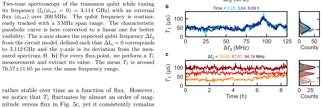
We developed an inorganic SiO2/Si3N4 on-chip stencil lithography mask for JJ fabrication. The stencil mask is resilient to aggressive cleaning agents and it withstands high temperatures up to 1200°C. We performed shadow evaporation of Al-based transmon qubits followed by stencil mask lift-off using vapor hydrofluoric acid, which selectively etches SiO2. We demonstrate average T1 ≈ 75 ± 11 μs over a 200 MHz frequency range in multiple cool-downs for one device, and T1 ≈ 44± 8 μs for a second device. These results confirm the compatibility of stencil lithography with state-of-the-art superconducting quantum devices.
What carries the argument
The SiO2/Si3N4 on-chip stencil mask for shadow evaporation of aluminum Josephson junctions, removed by selective vapor HF etching of the SiO2 layer.
If this is right
- The mask's high-temperature resilience opens avenues for exploring new JJ materials and interface optimization.
- The process remains compatible with aggressive surface cleaning agents that organic resists cannot tolerate.
- Achieved T1 values of 75 μs and 44 μs validate that the stencil approach reaches state-of-the-art coherence.
- The technique motivates further work on materials engineering, film deposition, and surface cleaning for qubits.
Where Pith is reading between the lines
- Removing organic resist residues may reduce a common source of decoherence and improve reproducibility across devices.
- The same stencil process could extend to other quantum circuits that require clean, high-temperature-tolerant fabrication steps.
- Selective lift-off might enable tighter control over junction geometry in multi-layer or 3D qubit architectures.
Load-bearing premise
The vapor hydrofluoric acid lift-off selectively etches the SiO2 without damaging the aluminum Josephson junctions or introducing new decoherence sources.
What would settle it
Fabricating identical transmons with the stencil method and measuring T1 values well below 40 μs or finding clear junction damage after the HF lift-off step.
Figures


read the original abstract
Improvements in circuit design and more recently in materials and surface cleaning have contributed to a rapid development of coherent superconducting qubits. However, organic resists commonly used for shadow evaporation of Josephson junctions (JJs) pose limitations due to residual contamination, poor thermal stability and compatibility under typical surface-cleaning conditions. To provide an alternative, we developed an inorganic SiO$_2$/Si$_3$N$_4$ on-chip stencil lithography mask for JJ fabrication. The stencil mask is resilient to aggressive cleaning agents and it withstands high temperatures up to 1200{\deg}C, thereby opening new avenues for JJ material exploration and interface optimization. To validate the concept, we performed shadow evaporation of Al-based transmon qubits followed by stencil mask lift-off using vapor hydrofluoric acid, which selectively etches SiO$_2$. We demonstrate average $T_1 \approx 75 \pm 11 \mu$s over a 200 MHz frequency range in multiple cool-downs for one device, and $T_1 \approx 44\pm 8 \mu$s for a second device. These results confirm the compatibility of stencil lithography with state-of-the-art superconducting quantum devices and motivate further investigations into materials engineering, film deposition and surface cleaning techniques.
Editorial analysis
A structured set of objections, weighed in public.
Referee Report
Summary. The manuscript introduces an inorganic SiO₂/Si₃N₄ on-chip stencil mask for shadow-evaporation fabrication of Al Josephson junctions in transmon qubits. The stencil is presented as an alternative to organic resists because it tolerates aggressive surface cleaning and temperatures up to 1200 °C. After vapor-HF lift-off, the authors report average T₁ ≈ 75 ± 11 μs over a 200 MHz range in multiple cool-downs for one device and T₁ ≈ 44 ± 8 μs for a second device, concluding that the process is compatible with state-of-the-art superconducting qubits.
Significance. If the central claim holds, the work provides a practical route to materials and interface studies that are currently blocked by organic-resist limitations. The reported coherence times are competitive with contemporary Al devices and constitute a direct experimental demonstration that the inorganic stencil plus vapor-HF lift-off can produce functional qubits.
major comments (2)
- [Results] Results section (and abstract): the claim that the measured T₁ values demonstrate compatibility with state-of-the-art devices rests on the premise that the stencil mask and vapor-HF lift-off introduce neither junction damage nor additional decoherence channels. No side-by-side control devices fabricated with conventional PMMA/MAA organic resists under otherwise identical conditions are reported, so the T₁ figures cannot be attributed specifically to the new process rather than to film quality, substrate preparation, or geometry that would be present in any fabrication run.
- [Methods] Methods / Fabrication section: post-lift-off junction characterization (I–V curves, critical-current density) and interface analysis (TEM/SEM) that would confirm unchanged junction properties and absence of etch-induced defects are not described. These data are load-bearing for the weakest assumption that vapor-HF selectively removes the SiO₂ without damaging the Al junctions.
minor comments (1)
- [Abstract] The abstract states averages and uncertainties but does not specify the number of individual qubits or the exact statistical procedure used to obtain the reported ±11 μs and ±8 μs values.
Simulated Author's Rebuttal
We thank the referee for the careful and constructive review of our manuscript. We address each major comment below and indicate the revisions planned for the next version of the manuscript.
read point-by-point responses
-
Referee: [Results] Results section (and abstract): the claim that the measured T₁ values demonstrate compatibility with state-of-the-art devices rests on the premise that the stencil mask and vapor-HF lift-off introduce neither junction damage nor additional decoherence channels. No side-by-side control devices fabricated with conventional PMMA/MAA organic resists under otherwise identical conditions are reported, so the T₁ figures cannot be attributed specifically to the new process rather than to film quality, substrate preparation, or geometry that would be present in any fabrication run.
Authors: We agree that the lack of side-by-side control devices fabricated with conventional organic resists prevents a direct, isolated attribution of the observed T1 performance to the stencil process alone. The manuscript demonstrates that the inorganic stencil enables fabrication of functional transmon qubits with T1 times (75 ± 11 μs and 44 ± 8 μs) that fall within the range of contemporary high-quality Al devices reported in the literature. We have revised the abstract and results section to clarify that these values establish compatibility and feasibility of the method rather than a quantitative comparison of process-induced effects. A sentence has been added noting that systematic comparative studies with organic-resist controls are planned for future work. revision: partial
-
Referee: [Methods] Methods / Fabrication section: post-lift-off junction characterization (I–V curves, critical-current density) and interface analysis (TEM/SEM) that would confirm unchanged junction properties and absence of etch-induced defects are not described. These data are load-bearing for the weakest assumption that vapor-HF selectively removes the SiO₂ without damaging the Al junctions.
Authors: We acknowledge that direct post-lift-off I–V characterization and TEM/SEM interface analysis would provide stronger confirmation that the vapor-HF step leaves the Al junctions intact. The present evidence for junction functionality is the successful qubit operation and measured coherence times. We have added a short paragraph in the methods section referencing the known high selectivity of vapor-HF for SiO2 over aluminum and have noted that dedicated electrical and microscopic characterization of junctions after lift-off will be included in follow-up studies. revision: partial
Circularity Check
No circularity: purely experimental fabrication and direct T1 measurements
full rationale
The manuscript reports an experimental process for fabricating Al transmon qubits via inorganic SiO2/Si3N4 stencil masks followed by vapor-HF lift-off, with results consisting solely of measured coherence times (average T1 ≈ 75 ± 11 μs and 44 ± 8 μs). No equations, first-principles derivations, fitted parameters, or predictions appear in the provided text; the T1 values are raw experimental outputs rather than quantities reduced by construction to inputs or self-citations. The work is self-contained against external benchmarks because the compatibility claim rests on direct comparison to state-of-the-art T1 values, not on any internal redefinition or load-bearing self-reference.
Axiom & Free-Parameter Ledger
axioms (1)
- domain assumption Vapor HF etching selectively removes the SiO2 layer without damaging the Al junctions or introducing additional loss mechanisms
Lean theorems connected to this paper
-
IndisputableMonolith/Foundation/RealityFromDistinction.leanreality_from_one_distinction unclear?
unclearRelation between the paper passage and the cited Recognition theorem.
We developed an inorganic SiO2/Si3N4 on-chip stencil lithography mask for JJ fabrication... vapor hydrofluoric acid lift-off
-
IndisputableMonolith/Cost/FunctionalEquation.leanwashburn_uniqueness_aczel unclear?
unclearRelation between the paper passage and the cited Recognition theorem.
average T1 ≈ 75 ± 11 μs ... confirm the compatibility of stencil lithography with state-of-the-art superconducting quantum devices
What do these tags mean?
- matches
- The paper's claim is directly supported by a theorem in the formal canon.
- supports
- The theorem supports part of the paper's argument, but the paper may add assumptions or extra steps.
- extends
- The paper goes beyond the formal theorem; the theorem is a base layer rather than the whole result.
- uses
- The paper appears to rely on the theorem as machinery.
- contradicts
- The paper's claim conflicts with a theorem or certificate in the canon.
- unclear
- Pith found a possible connection, but the passage is too broad, indirect, or ambiguous to say the theorem truly supports the claim.
Forward citations
Cited by 2 Pith papers
-
Resist-free shadow deposition using silicon trenches for Josephson junctions in superconducting qubits
A resist-free silicon-trench shadow deposition method fabricates Al-AlOx-Al Josephson junctions and qubits with median relaxation times up to 184 microseconds and minimal substrate-metal contamination.
-
Resist-free shadow deposition using silicon trenches for Josephson junctions in superconducting qubits
Resist-free shadow deposition via etched silicon trenches produces Al-AlOx-Al Josephson junctions with median qubit energy relaxation times of 184 microseconds and minimal substrate-metal interface contamination.
Reference graph
Works this paper leans on
-
[1]
On-chip stencil lithography for superconducting qubits
of the desired circuit element geometry. However, in the case of lift-off, the presence of the relatively fragile polymer mask limits pre-growth cleaning methods such as hydrofluoric acid (HF) treatments and deposition tem- peratures above ∼ 300°C. This could lead to amorphous or poly-crystalline layers [41, 42], oxidized substrate sur- faces [21, 23] and...
work page internal anchor Pith review Pith/arXiv arXiv doi:10.5281/zenodo.15976967 2025
-
[2]
Material evaporation
-
[3]
On-chip stencil fabrication details
Stencil lift-off a b c Low angle deposition High angle deposition Deposition Deposition Si3N4 SiO2 S Sapphire hole Blocked Deposition Deposition Si3N4 SiO2 S Sapphire Al dots Deposition-free hole 100 nm100 nm α Figure A1. On-chip stencil fabrication details. a) Three main steps of the stencil transmon qubit fabrication: 1) stencil mask preparation and int...
work page 2000
-
[4]
A. I. Braginski, Journal of Superconductivity and Novel Magnetism 32, 23 (2019)
work page 2019
-
[5]
A. Peacock, P. Verhoeve, N. Rando, A. van Dordrecht, B. G. Taylor, C. Erd, M. A. C. Perryman, R. Venn, J. Howlett, D. J. Goldie, J. Lumley, and M. Wallis, Na- ture 381, 135 (1996)
work page 1996
-
[6]
P. K. Day, H. G. LeDuc, B. A. Mazin, A. Vayonakis, and J. Zmuidzinas, Nature 425, 817 (2003)
work page 2003
-
[7]
F. Arute, K. Arya, R. Babbush, D. Bacon, J. Bardin, R. Barends, R. Biswas, S. Boixo, F. Brandao, D. Buell, B. Burkett, Y. Chen, J. Chen, B. Chiaro, R. Collins, W. Courtney, A. Dunsworth, E. Farhi, B. Foxen, A. Fowler, C. M. Gidney, M. Giustina, R. Graff, K. Guerin, S. Habegger, M. Harrigan, M. Hartmann, A. Ho, M. R. Hoffmann, T. Huang, T. Humble, S. Isako...
work page 2019
-
[8]
P. Jurcevic, A. Javadi-Abhari, L. S. Bishop, I. Lauer, D. F. Bogorin, M. Brink, L. Capelluto, O. G¨ unl¨ uk, T. Itoko, N. Kanazawa, A. Kandala, G. A. Keefe, K. Kr- sulich, W. Landers, E. P. Lewandowski, D. T. McClure, G. Nannicini, A. Narasgond, H. M. Nayfeh, E. Pritchett, M. B. Rothwell, S. Srinivasan, N. Sundaresan, C. Wang, K. X. Wei, C. J. Wood, J.-B....
work page 2021
-
[9]
R. Acharya, D. A. Abanin, L. Aghababaie-Beni, I. Aleiner, T. I. Andersen, M. Ansmann, F. Arute, K. Arya, A. Asfaw, N. Astrakhantsev, et al. , Nature (2024)
work page 2024
-
[10]
M. H. Devoret and R. J. Schoelkopf, Science 339, 1169 (2013)
work page 2013
-
[11]
Siddiqi, Nature Reviews Materials 6, 1 (2021)
I. Siddiqi, Nature Reviews Materials 6, 1 (2021)
work page 2021
-
[12]
A. Wallraff, D. Schuster, A. Blais, L. Frunzio, R. Huang, J. Majer, S. Kumar, S. Girvin, and R. Schoelkopf, Na- ture (2004)
work page 2004
-
[13]
J. Koch, T. Yu, J. Gambetta, A. Houck, D. Schus- ter, J. Majer, A. Blais, M. Devoret, S. Girvin, and R. Schoelkopf, Physical Review A 76 (2007)
work page 2007
-
[14]
J. Q. You, X. Hu, S. Ashhab, and F. Nori, Phys. Rev. B 75, 140515 (2007)
work page 2007
-
[15]
R. Barends, J. Kelly, A. Megrant, D. Sank, E. Jef- frey, Y. Chen, Y. Yin, B. Chiaro, J. Mutus, C. Neill, P. O’Malley, P. Roushan, J. Wenner, T. White, A. Cle- land, and J. Martinis, Physical review letters 111, 080502 (2013)
work page 2013
- [16]
-
[17]
B. N. Long, Y.-H. Lin, A. Somoroff, R. Mencia, N. Grabon, and V. Manucharyan, Physical Review X 9 (2019)
work page 2019
-
[18]
J. Martinis, K. Cooper, R. McDermott, M. Steffen, M. Ansmann, K. Osborn, K. Cicak, S. Oh, D. Pappas, R. Simmonds, and C. Yu, Physical Review Letters 95, 210503 (2005)
work page 2005
-
[19]
S. Oh, K. Cicak, J. S. Kline, M. A. Sillanp¨ a¨ a, K. D. Osborn, J. D. Whittaker, R. W. Simmonds, and D. P. Pappas, Phys. Rev. B 74, 100502 (2006)
work page 2006
-
[20]
J. Lisenfeld, A. Bilmes, A. Megrant, R. Barends, J. Kelly, P. Klimov, G. Weiss, J. Martinis, and A. Ustinov, npj Quantum Information 5, 105 (2019)
work page 2019
-
[21]
C. Quintana, A. Megrant, Z. Chen, A. Dunsworth, B. Chiaro, R. Barends, B. Campbell, Y. Chen, I.- C. Hoi, E. Jeffrey, J. Kelly, J. Mutus, P. O’Malley, C. Neill, P. Roushan, D. Sank, A. Vainsencher, J. Wen- ner, T. White, and J. Martinis, Applied Physics Letters 105 (2014)
work page 2014
-
[22]
C. Wang, C. Axline, Y. Gao, T. Brecht, L. Frunzio, M. Devoret, and R. Schoelkopf, Applied Physics Letters 107 (2015)
work page 2015
-
[23]
O. Dial, D. McClure, S. Poletto, J. Gambetta, D. Abra- ham, J. Chow, and M. Steffen, Superconductor Science and Technology 29 (2015)
work page 2015
-
[24]
J. Gambetta, C. Murray, Y. Fung, D. McClure, O. Dial, W. Shanks, J. Sleight, and M. Steffen, IEEE Transac- tions on Applied Superconductivity PP (2016)
work page 2016
-
[25]
J. Bizn´ arov´ a, A. Osman, E. Rehnman, L. Chayanun, C. Kriˇ zan, P. Malmberg, M. Rommel, C. Warren, P. Dels- ing, A. Yurgens, J. Bylander, and A. Fadavi Roudsari, npj Quantum Information 10, 78 (2024)
work page 2024
- [26]
- [27]
- [28]
-
[29]
C. Wang, X. Li, H. Xu, Z. Li, J. Wang, Z. Yang, Z. Mi, X. Liang, T. Su, Y. Chuhong, G. Wang, W. Wang, Y. Li, M. Chen, C. Li, K. Linghu, J. Han, Y. Zhang, Y. Feng, and H. Yu, npj Quantum Information 8 (2022)
work page 2022
-
[30]
Bal et al., npj Quantum Inf.10, 43 (2024), 2304.13257 [quant-ph]
M. Bal et al., npj Quantum Inf.10, 43 (2024), 2304.13257 [quant-ph]
-
[31]
G. J. Dolan, Applied Physics Letters 31, 337 (1977)
work page 1977
-
[32]
N. Muthusubramanian, M. Finkel, P. Duivestein, C. Zachariadis, S. L. M. van der Meer, H. M. Veen, M. W. Beekman, T. Stavenga, A. Bruno, and L. DiCarlo, Quan- tum Science and Technology 9, 025006 (2024)
work page 2024
-
[33]
A. A. Pishchimova, N. S. Smirnov, D. A. Ezenkova, E. A. Krivko, E. V. Zikiy, D. O. Moskalev, A. I. Ivanov, N. D. Korshakov, and I. A. Rodionov, Scientific Reports 13, 6772 (2023)
work page 2023
-
[34]
J. Van Damme, S. Massar, R. Acharya, T. Ivanov, D. Perez Lozano, Y. Canvel, M. Demarets, et al. , Na- ture 634, 74 (2024)
work page 2024
- [35]
-
[36]
G. Marchegiani, L. Amico, and G. Catelani, PRX Quan- tum 3, 040338 (2022)
work page 2022
-
[37]
P. Kamenov, T. DiNapoli, M. Gershenson, and S. Chakram, arXiv preprint arXiv:2309.02655 (2023)
-
[38]
M. McEwen, K. C. Miao, J. Atalaya, A. Bilmes, A. Crook, J. Bovaird, J. M. Kreikebaum, N. Zo- brist, E. Jeffrey, B. Ying, A. Bengtsson, H.-S. Chang, A. Dunsworth, J. Kelly, Y. Zhang, E. Forati, R. Acharya, J. Iveland, W. Liu, S. Kim, B. Burkett, A. Megrant, Y. Chen, C. Neill, D. Sank, M. Devoret, and A. Oprem- cak, Phys. Rev. Lett. 133, 240601 (2024)
work page 2024
- [39]
-
[40]
S. Kim, H. Terai, T. Yamashita, W. Qiu, T. Fuse, F. Yoshihara, S. Ashhab, K. Inomata, and K. Semba, Communications Materials 2, 98 (2021)
work page 2021
- [41]
-
[42]
J. M. Kreikebaum, K. P. O’Brien, A. Morvan, and I. Sid- diqi, Superconductor Science and Technology33, 06LT02 (2020)
work page 2020
- [43]
-
[44]
L. Zeng, S. Nik, T. Greibe, P. Krantz, C. Wilson, P. Dels- ing, and E. Olsson, Journal of Physics D: Applied Physics 48 (2015)
work page 2015
-
[45]
L. Zeng, D. Tran, C.-W. Tai, G. Svensson, and E. Olsson, Scientific Reports 6, 29679 (2016)
work page 2016
-
[46]
I. M. Pop, T. Fournier, T. Crozes, F. Lecocq, I. Matei, B. Pannetier, O. Buisson, and W. Guichard, Journal of Vacuum Science & Technology B 30, 010607 (2012)
work page 2012
-
[47]
V. Milchakov, Optimized transmon molecule for high fi- delity quantum non demolition readout using cross-Kerr coupling, Theses, Universit´ e Grenoble Alpes (2022)
work page 2022
-
[48]
N. Johnson, Atomic Layer Etching of Metal Films, Metal Nitrides, and Metal Oxides with BCl3 and HF/XeF2 , Ph.D. thesis, University of Colorado at Boulder (2019)
work page 2019
-
[49]
O. Vazquez-Mena, L. Gross, S. Xie, L. Villanueva, and J. Brugger, Microelectronic Engineering 132, 236 (2015), micro and Nanofabrication Breakthroughs for Electron- ics, MEMS and Life Sciences
work page 2015
-
[50]
I. Tsioutsios, K. Serniak, S. Diamond, V. V. Sivak, Z. Wang, S. Shankar, L. Frunzio, R. J. Schoelkopf, and M. H. Devoret, AIP Advances 10, 065120 (2020)
work page 2020
-
[51]
P. Welander, V. Bolkhovsky, T. Weir, M. Gouker, and W. Oliver, arXiv (2012)
work page 2012
-
[52]
T. Hoss, C. Strunk, and C. Sch¨ onenberger, Microelec- tronic engineering 46, 149 (1999)
work page 1999
-
[53]
P. Sch¨ uffelgen, D. Rosenbach, C. Li, T. Schmitt, M. Schleenvoigt, A. R. Jalil, S. Schmitt, J. K¨ olzer, M. Wang, B. Bennemann, U. Parlak, L. Kibkalo, S. Trel- lenkamp, T. Grap, D. Meertens, M. Luysberg, G. Mus- sler, J. Berenschot, N. Tas, and D. Gr¨ utzmacher, Nature Nanotechnology 14, 1 (2019)
work page 2019
-
[54]
T. W. Schmitt, M. R. Connolly, M. Schleenvoigt, C. Liu, O. Kennedy, J. M. Ch´ avez-Garcia, A. R. Jalil, et al. , Nano letters 22, 2595 (2022)
work page 2022
-
[55]
A. Witvrouw, B. Bois, P. De Moor, A. Verbist, C. Van Hoof, H. Bender, and C. Baert, Proceedings of SPIE - The International Society for Optical Engineering 4174 (2000)
work page 2000
-
[56]
A. Dunsworth, R. Barends, Y. Chen, Z. Chen, B. Chiaro, A. Fowler, B. Foxen, E. Jeffrey, J. Kelly, P. V. Klimov, E. Lucero, J. Y. Mutus, M. Neeley, C. Neill, C. Quin- tana, P. Roushan, D. Sank, A. Vainsencher, J. Wenner, T. C. White, H. Neven, J. M. Martinis, and A. Megrant, Applied Physics Letters 112, 063502 (2018)
work page 2018
- [57]
- [58]
-
[59]
A. Kou, W. C. Smith, U. Vool, I. M. Pop, K. M. Sliwa, M. Hatridge, L. Frunzio, and M. H. Devoret, Phys. Rev. Appl. 9, 064022 (2018)
work page 2018
-
[60]
L. Gr¨ unhaupt, M. Spiecker, D. Gusenkova, N. Maleeva, S. Skacel, I. Takmakov, F. Valenti, P. Winkel, H. Rotzinger, W. Wernsdorfer, A. Ustinov, and I. Pop, Nature Materials 18 (2019)
work page 2019
-
[61]
T. Thorbeck, A. Eddins, I. Lauer, D. T. McClure, and M. Carroll, PRX Quantum 4, 020356 (2023)
work page 2023
-
[62]
M. Spiecker, P. Paluch, N. Gosling, N. Drucker, S. Matityahu, D. Gusenkova, S. G¨ unzler, D. Rieger, I. Takmakov, F. Valenti, et al., Nature Physics 19, 1320 (2023)
work page 2023
-
[63]
J. Martinis, M. Ansmann, and J. Aumentado, Physical Review Letters 103, 097002 (2009)
work page 2009
-
[64]
I. Pop, K. Geerlings, G. Catelani, R. Schoelkopf, L. Glaz- man, and M. Devoret, Nature 508, 369 (2014)
work page 2014
-
[65]
P. V. Klimov, J. Kelly, Z. Chen, M. Neeley, A. Megrant, B. Burkett, R. Barends, K. Arya, B. Chiaro, Y. Chen, A. Dunsworth, A. Fowler, et al. , Phys. Rev. Lett. 121, 090502 (2018)
work page 2018
- [66]
-
[67]
S. Martinussen, E. Berenschot, D. Bonneville, K. Wang, M. Dijkstra, N. Tas, S. Garc´ ıa-Blanco, and R. Tiggelaar, Optics express 32, 36835 (2024)
work page 2024
-
[68]
AR-P 6200.09 – CSAR 62 Series E- Beam Resist,
Allresist GmbH, “AR-P 6200.09 – CSAR 62 Series E- Beam Resist,” (2025)
work page 2025
-
[69]
AR-PC 5090.02 – Electra 92 Protective Coating,
Allresist GmbH, “AR-PC 5090.02 – Electra 92 Protective Coating,” (2025)
work page 2025
-
[70]
Espacer ™ 300Z Conductive Poly- mer,
Resonac Corporation, “Espacer ™ 300Z Conductive Poly- mer,” (2025)
work page 2025
- [71]
-
[72]
T. J. Smart, D. Y. Kim, and W. Braun, Journal of Vac- uum Science and Technology B 42, 062204 (2024)
work page 2024
-
[73]
D. Y. Kim, T. J. Smart, J. Mannhart, and W. Braun, Crystal Growth & Design 23, 8087 (2023)
work page 2023
-
[74]
R. J. Carter, J. R. Hauser, and R. J. Nemanich, Journal of The Electrochemical Society 147, 3512 (2000)
work page 2000
- [75]
-
[76]
S. Guillemin, P. Mumbauer, H. Radtke, M. Fimberger, S. Fink, J. Kraxner, A. Faes, and J. Siegert, Journal of Microelectromechanical Systems 28, 717 (2019)
work page 2019
-
[77]
Primaxx ® uEtch – HF Vapor Etch Systems,
KLA Corporation, “ Primaxx ® uEtch – HF Vapor Etch Systems,” (2025)
work page 2025
discussion (0)
Sign in with ORCID, Apple, or X to comment. Anyone can read and Pith papers without signing in.