REVIEW 3 major objections 5 minor 15 references
Approaching transform-limited linewidths in telecom-wavelength transitions of ungated quantum dots
T0 review · 3 major / 5 minor · reviewed 2026-08-05 · deepseek-v4-flash
Pith's one-line read The paper claims that a GaP interlayer growth scheme produces telecom C-band InAs/InP quantum dots whose low-power linewidths approach the transform-limited value: a mean of 12.1 ± 6.7 ΓTL and a best of 2.8 ± 1.8 ΓTL.
desk verdict A useful growth advance with honest reporting, but the headline linewidths are model-extrapolated, not measured—treat the 2.8 ΓTL claim as conditional. read the letter →
The pith
A machine-rendered reading of the paper's core claim, the machinery that carries it, and where it could break.
The reading
What carries the argument
The load-bearing object is the two-level thermal-bath model expressed in Eq. S.24, Γmeas(P) = ΓTL[1 + (P/Psat)^n] + Γdp/2π, which converts high-power etalon linewidths into zero-power linewidths by assuming a pump rate Px(P) = (ΓTL/2)(P/Psat)^n and a power-independent pure dephasing rate Γdp. The growth-side mechanism is the pseudomorphic GaP interlayer that blocks As/P exchange and keeps the surface smooth, producing highly symmetric dots with low density and small fine-structure splitting.
What would settle it
Measure the X* linewidth of several dots at excitation powers from ~0.01 Psat to Psat with the etalon, deconvolving its instrument response, and compare the power dependence to Eq. S.24. If the linewidth at low power does not approach the extrapolated values within error, or if the curvature deviates from the assumed [1 + (P/Psat)^n] form with constant offset, then the 12.1 and 2.8 ΓTL numbers are model artifacts. A second check is a direct, higher-resolution lifetime measurement to replace the upper-limit decay time used to set ΓTL.
Extended reading notes
Core claim
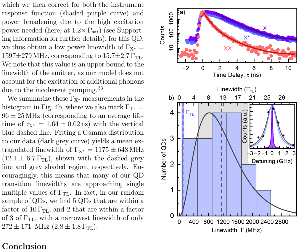
The paper's claim is that adding a 0.4 nm pseudomorphic GaP interlayer between the InP substrate and the InAs quantum-dot layer blocks arsenic–phosphorus exchange during Stranski–Krastanov growth, and that this simple growth change produces telecom C-band dots whose low-power transition linewidths are close to the fundamental transform limit. Under continuous-wave excitation at 965 nm (above the band gap) into the wetting layer, with no electric gate, no resonant drive, and only a weak mirror for collection, dots measured with a scanning etalon yield extrapolated zero-power linewidths with a statistical mean of 12.1 ± 6.7 ΓTL and a best case of 2.8 ± 1.8 ΓTL. The dots also show aspect ratios
Load-bearing premise
The load-bearing premise is that each dot's linewidth grows with laser power in the smooth way the thermal-bath model assumes, with the environment's added broadening staying constant at all powers; this extrapolation is not checked by measuring one dot's width at many powers, and it ignores extra blurring from phonons.
Editorial extensions
If this is right
- Above-band, ungated, bulk-embedded C-band dots can be within a few times the lifetime limit, so near-transform-limited telecom photons no longer require gating, resonant driving, or cavity enhancement.
- The GaP interlayer decouples dot density from dot quality, allowing sparse samples (down to ~2 µm−2) to be grown without sacrificing symmetry—useful for integration and device isolation.
- Small fine-structure splitting (25 ± 4 µeV) suggests the same dots can act as sources of polarization-entangled photon pairs in the telecom C-band.
- Because the reported linewidths are upper bounds, a model that includes phonon-induced broadening would likely place the best dots even closer to ΓTL than 2.8 appears.
- A random sample of these dots contains several near-transform-limited emitters, and the rest remain compatible with established Purcell, resonant-excitation, or gating techniques.
Reading between the lines
- Because the quoted decay times are explicitly upper limits on the radiative lifetime, the true transform-limited width is probably larger than the 96 MHz used here; if so, the real linewidth ratios are smaller (better) than the reported multiples, and the best dot may be even closer to lifetime-limited emission.
- A direct linewidth-versus-power sweep on a single dot down to a few percent of Psat would test whether Eq. S.24 truly describes these dots; the paper does not report such a sweep, so the strongest version of the claim rests on that unmeasured curve.
- The GaP-interlayer mechanism—blocking group-V intermixing—should transfer to other lattice-mismatched quantum-dot systems where surface roughening and density control set the linewidth floor.
- If phonon generation under above-band pumping is the remaining broadening source, resonantly exciting these same dots or adding a gate should push them below the 4 ΓTL benchmark; that is a testable next step.
Editorial analysis
A structured set of objections, weighed in public.
Referee Report
Summary. The paper reports a modified chemical-beam-epitaxy growth protocol for InAs/InP quantum dots emitting in the telecom C-band, in which a thin GaP interlayer suppresses As/P intermixing. The authors characterize the resulting dots by AFM, micro-PL, polarization-resolved spectroscopy, power-dependent measurements, time-resolved PL, and g(2) correlation measurements. The central claim is that these ungated, bulk, above-band-excited dots have low-power linewidths approaching the transform limit, with a statistical mean of 12.1 ± 6.7 Γ_TL and a best value of 2.8 ± 1.8 Γ_TL. These low-power linewidths are not measured directly; they are extrapolated from etalon linewidths taken at 1–6 × P_sat using the power-broadening model of Eq. S.24.
Significance. If established, the claim would be noteworthy: it would demonstrate near-transform-limited C-band emission from ungated, bulk, above-band-excited quantum dots, a regime where previous reports are typically 50–100 Γ_TL, and it would be competitive with gated, resonant, cavity-enhanced systems. The growth results themselves are also useful: the GaP interlayer produces low-density, highly symmetric dots with fine-structure splittings down to 25 ± 4 µeV and a raw g(2)(0) of 0.012 ± 0.007, and the authors are transparent about measurement limitations. However, the central quantitative claim depends on a power-broadening correction that is not validated on these samples, so the significance of the headline numbers is currently conditional on that model.
major comments (3)
- [Supporting Information, 'Quantum Dot Linewidths', Eq. S.24] The zero-power linewidths in Fig. 4b are not measured but extrapolated from a single high-power etalon measurement per dot (taken at 1–6 × P_sat) using Eq. S.24. That equation assumes a two-level system with power-independent pure dephasing Γ_dp and a pump rate P_x(P) = (Γ_TL/2)(P/P_sat)^n, with per-dot fitted P_sat and n. The paper reports no linewidth-versus-power sweep on these dots that would validate this functional form, and the model is taken from prior nanowire work (ref. 36). If the actual power broadening is shallower or steeper than Eq. S.24, the reported mean and best linewidths change. A single representative Γ(P) dataset, or an independent verification of Eq. S.24 on at least one dot, is needed to support the central claim.
- [Results, 'Analysis of single emission lines' and Eq. S.24] The decay times are explicitly described as upper limits because carrier capture/relaxation is not included in the lifetime fits. Since Γ_TL = 1/(2πT1), an upper-limit T1 gives a lower-limit Γ_TL, so the quoted multiples Γ/Γ_TL systematically understate the true ratio. The paper labels the extrapolated linewidths as upper bounds, but that does not imply an upper bound on Γ/Γ_TL. This should be acknowledged, and the absolute frequency values should be emphasized alongside the Γ_TL multiples.
- [Fig. 4b and summary statistics] The best-case value of 2.8 ± 1.8 Γ_TL has a relative uncertainty of about 60%, and the mean value of 12.1 ± 6.7 Γ_TL has a similar spread. After etalon deconvolution and the model correction, the histogram in Fig. 4b therefore does not currently establish that a substantial fraction of dots are within a few Γ_TL. Reporting the raw etalon linewidths and the individual corrected values, with a clear propagation of the P_sat, n, T1, and etalon-resolution uncertainties, would make the statistical claim more robust.
minor comments (5)
- [Fig. 4b caption] The text says '17 different QDs' in one place and '18 randomly selected QDs' in another; the histogram caption also says 18. Please reconcile these numbers.
- [References] Several references contain corrupted strings, e.g., 'Kardyna/suppress l' in ref. 6 and 'Musia/suppress l' in refs. 11 and 15. These need to be cleaned.
- [Supporting Information, 'Additional Optical Measurements on Non-Flip-bonded QDs'] The text refers to 'Fig. S3c' when discussing polarization maps, but the relevant panel appears to be Fig. S2c. Please check cross-references.
- [Methods, 'QD Sample Growth'] The flip-bonded sample is called 'sample D' in the main text, while the supporting-information growth table lists samples S, A, B, and C. Clarify the correspondence.
- [Supporting Information, Eq. S.24] The derivation labels Γ_2 as the HWHM and then converts via Γ_meas = Γ_2/π; this is correct for a Lorentzian in angular frequency but the notation is not defined in the main text. A one-line definition of Γ_2 in the main text would avoid confusion.
Circularity Check
No significant circularity: the low-power linewidths are model-based extrapolations from independently measured high-power widths, lifetimes, and saturation fits, not fitted inputs or renamed predictions.
full rationale
The paper's central quantitative claim—mean low-power linewidth 12.1±6.7 ΓTL and best 2.8±1.8 ΓTL—is not obtained by fitting the low-power linewidth itself. For each dot, the measured high-power etalon linewidth, the measured lifetime T1, and the intensity-fit saturation parameters Psat and n are inserted into Eq. S.24. The pure-dephasing contribution Γdp is then solved from Γmeas(P) = ΓTL[1+(P/Psat)^n] + Γdp/(2π), and the zero-power width is ΓTL + Γdp/(2π). Algebraically this equals the measured high-power width minus a model correction ΓTL(P/Psat)^n. That correction is computed from independent inputs (lifetime and saturation fit), not from the target linewidth, so the result is an extrapolation rather than a circular fit. The thermal-bath model underlying Eq. S.24 is cited to Yao et al. (main-text ref. 33; SI ref. 8), an external source, not to the authors' own prior work. The self-citations (Laferriere et al., ref. 36; Wakileh et al., ref. 23; Reimer et al., ref. 27) are used for background, complex identification, or the explicit caveat that the model does not include pump-power-dependent phonon excitation; none of these carries the central derivation. The authors themselves repeatedly call the extracted linewidth an upper bound because of the neglected phonon mechanism, which is a limitation on certainty but not circularity. Likewise, the statement that the measured decay times are upper limits affects the ΓTL normalization and the interpretation of the multiples, but does not make the reported values equal to an input by construction. The comparison to prior work in Table S3 uses the same extrapolated values, but the comparison is not the derivation. Overall, the central observation is independent of the cited prior results, and the self-citations are not load-bearing. Score 1 reflects only minor non-load-bearing self-citations; the core derivation is self-contained and not circular.
Assumptions & free parameters
free parameters (3)
- saturation power Psat (X*, QD3) =
16.4 ± 2.7 µW
- power-law exponent n (X*, QD3) =
1.09 ± 0.04; mean n = 1.15 ± 0.04
- pure dephasing rate Γdp per QD =
1495 ± 278 MHz for QD3
assumptions (5)
- domain assumption Quantum dot is a two-level system weakly coupled to a thermal bath obeying a Born-Markov master equation with Lindblad terms for incoherent pump, decay, and pure dephasing.
- ad hoc to paper Effective pump rate is a power law Px(P) = (ΓTL/2)(P/Psat)^n, calibrated so Px = ΓTL/2 at Psat.
- domain assumption Measured TRPL decay time T1 gives the transform-limited linewidth ΓTL = 1/(2πT1).
- domain assumption The etalon instrument response is Lorentzian and the observed linewidth is the sum of QD and IRF widths.
- standard math Quantum regression theorem for two-time correlations.
Cite this review
Pith. "Pith review of Approaching transform-limited linewidths in telecom-wavelength transitions of ungated quantum dots." pith.science (2026). https://pith.science/paper/K6WO6HXG
@misc{pith2026250902320,
  author       = {Pith},
  title        = {Pith review of: Approaching transform-limited linewidths in telecom-wavelength transitions of ungated quantum dots},
  year         = {2026},
  howpublished = {\url{https://pith.science/paper/K6WO6HXG}},
  note         = {Machine review of arXiv:2509.02320}
}
abstract
Highly coherent quantum emitters operating in the telecommunication C-band (1530 - 1565nm), where ultra-low-loss fibers and photonic circuits are available, are crucial to the development of scalable quantum technologies. In this work, we report on a modified Stranski-Krastanov growth scheme using chemical beam epitaxy to enable the generation of high-quality InAs/InP quantum dots, characterized by near-transform-limited linewidths ($\Gamma_{\mathrm{TL}}$). We demonstrate the growth of highly-symmetric quantum dots with aspect ratios >0.8 and densities ranging from 2 to 22$\,\mu$m$^{-2}$. Optical characterization of these sources reveal fine-structure splittings down to $25\pm4\,\mu$eV and a single-photon purity of $g^{(2)}(0) = 0.012\pm\mathrm{0.007}$, confirming the quality of these dots. Further, using an etalon to measure the linewidth, in combination with rigorous modelling, we find an upper-bound to the mean, low-power linewidths of only $12.1\pm 6.7\,\Gamma_\mathrm{TL}$ and, in the best case, $2.8\pm 1.8\,\Gamma_\mathrm{TL}$. These results represent a significant step in the development of telecom-wavelength quantum light sources which are essential for complex quantum networks and devices.
Figures


Figures from the paper (1 more)
Reference graph
Works this paper leans on
-
[1]
J.; Kaminska, K.; Barrios, P.; Lu, Z.; Liu, J
Poole, P. J.; Kaminska, K.; Barrios, P.; Lu, Z.; Liu, J. Growth of InA s/InP-based quantum dots for 1.55 um laser applications. J. Cryst. Growth 2009, 311, 1482–1486
work page 2009
-
[2]
Laferri` ere, P.; Yeung, E.; Korkusinski, M.; Poole, P. J.; Williams, R. L.; Dalacu, D.; Manalo, J.; Cygorek, M.; Altintas, A.; Hawrylak, P. Systematic Study of the Emission Spectra of Nanowire Quantum Dots. Applied Physics Letters 2021, 118, 161107
work page 2021
-
[3]
H.; Malko, A.; Pelucchi, E.; Oberli, D
Baier, M. H.; Malko, A.; Pelucchi, E.; Oberli, D. Y.; Kapon, E. Quantum-Dot Exciton Dynamics Probed by Photon-Correlation Spectroscopy. 73, 205321
-
[4]
Sallen, G.; Tribu, A.; Aichele, T.; Andr´ e, R.; Besombes, L.; Bougero l, C.; Tatarenko, S.; Kheng, K.; Poizat, J. Ph. Exciton Dynamics of a Single Quantum Dot Embedded in a Nanowire. Physical Review B 2009, 80, 085310
work page 2009
-
[5]
Anderson, M.; M¨ uller, T.; Skiba-Szymanska, J.; Krysa, A. B.; Huw er, J.; Stevenson, R. M.; Heffernan, J.; Ritchie, D. A.; Shields, A. J. Coherence in Single Photon Emission from Droplet Epitaxy and Stranski–Krastanov Quantum Dots in the Telecom C-band. Applied Physics Letters 2021, 118, 014003
work page 2021
-
[6]
C.; Scholz, S.; S¨ ollner, I.; Ritzmann, J.; Denneulin, T.; Kov´ acs, A.; Kardyna/suppress l, B
L¨ obl, M. C.; Scholz, S.; S¨ ollner, I.; Ritzmann, J.; Denneulin, T.; Kov´ acs, A.; Kardyna/suppress l, B. E.; Wieck, A. D.; Ludwig, A.; Warburton, R. J. Excitons in InGaAs Quantu m Dots without Electron Wetting Layer States. Communications Physics 2019, 2, 93
work page 2019
-
[7]
B.; Haffouz, S.; Lapointe, J.; Poole, P
Laferri` ere, P.; Yin, A.; Yeung, E.; Kusmic, L.; Korkusinski, M.; Rasekh, P.; Northeast, D. B.; Haffouz, S.; Lapointe, J.; Poole, P. J.; Williams, R. L.; Dalacu, D. Approa ching transform- limited photons from nanowire quantum dots using excitation above t he band gap. Phys. Rev. B 2023, 107, 155422
work page 2023
-
[8]
Yao, P.; Pathak, P. K.; Illes, E.; Hughes, S.; M¨ unch, S.; Reitzenstein, S.; Franeck, P.; L¨ offler, A.; Heindel, T.; H¨ ofling, S.; Worschech, L.; Forchel, A. Nonlinear Photoluminescence Spectra from a Quantum-Dot–Cavity System: Interplay of Pump-Induced Stimu lated Emission and Anhar- monic Cavity QED. Physical Review B 2010, 81, 033309
work page 2010
Show all 15 references
-
[9]
Steck, D. A. Quantum and Atom Optics. Lecture notes, available online, 2007; http://steck. us/teaching, Revision 0.9.12 (16 July 2014)
2007
-
[10]
A.; Holewa, P.; Zieba-Ost´ oj, E.; Wasiluk, M.; von Helve rsen, M.; Sakanas, A.; Huck, A.; Yvind, K.; Gregersen, N.; Musia/suppress l, A.; Syperek, M.; Semenova, E.; Heindel, T
Vajner, D. A.; Holewa, P.; Zieba-Ost´ oj, E.; Wasiluk, M.; von Helve rsen, M.; Sakanas, A.; Huck, A.; Yvind, K.; Gregersen, N.; Musia/suppress l, A.; Syperek, M.; Semenova, E.; Heindel, T. On- Demand Generation of Indistinguishable Photons in the Telecom C-Ba nd Using Quantum ...
2024
-
[11]
Holewa, P.; Vajner, D. A.; Zieba-Ost´ oj, E.; Wasiluk, M.; Ga´ al, B.;Sakanas, A.; Burakowski, M.; Mrowi´ nski, P.; Krajnik, B.; Xiong, M.; Yvind, K.; Gregersen, N.; Musia/suppress l, A.; Huck, A.; Hein- del, T.; Syperek, M.; Semenova, E. High-throughput quantum phot onic devi...
2024
-
[12]
L.; Brash, A
Phillips, C. L.; Brash, A. J.; Godsland, M.; Martin, N. J.; Foster, A.; Tomlinson, A.; Dost, R.; Babazadeh, N.; Sala, E. M.; Wilson, L.; Heffernan, J.; Skolnick, M. S.; Fo x, A. M. Purcell- enhanced single photons at telecom wavelengths from a quantum do t in a photonic crystal...
2024
-
[13]
H.; Harper, S.; Lee, C.-M.; Kim, K.-Y.; Buyukkaya, M
Rahaman, M. H.; Harper, S.; Lee, C.-M.; Kim, K.-Y.; Buyukkaya, M. A.; Patel, V. J.; Hawkins, S. D.; Kim, J.-H.; Addamane, S.; Waks, E. Efficient, Indistingu ishable Telecom C- Band Photons using a Tapered Nanobeam Waveguide. ACS Publications 2024,
2024
-
[14]
M.; Skiba-Szymanska, J.; Ritc hie, D
Wells, L.; M¨ uller, T.; Stevenson, R. M.; Skiba-Szymanska, J.; Ritc hie, D. A.; Shields, A. J. Coherent light scattering from a telecom C-band quantum dot. Nat. Commun. 2023, 14, 8371
2023
-
[15]
P.; Sek, G.; Benyoucef, M
Musia/suppress l, A.; Holewa, P.; Wyborski, P.; Syperek, M.; Kors, A.; Reithmaier, J. P.; Sek, G.; Benyoucef, M. High-Purity Triggered Single-Photon Emission from Symmetric Single InAs/InP Quantum Dots around the Telecom C-Band Window.Adv. Quantum Technol. 2020, 3, 1900082. 13
2020
Reviewed August 5, 2026 · model on record in the stance chip above.
Discussion (0). Continue with ORCID to comment.