Optically programmable and erasable cryogenic flash memory on an undoped Si/SiGe heterostructure
Pith reviewed 2026-06-28 18:17 UTC · model grok-4.3
The pith
High interface trap density locks threshold voltage in Si/SiGe transistors for optical non-volatile memory at 1.5 K.
A machine-rendered reading of the paper's core claim, the machinery that carries it, and where it could break.
Core claim
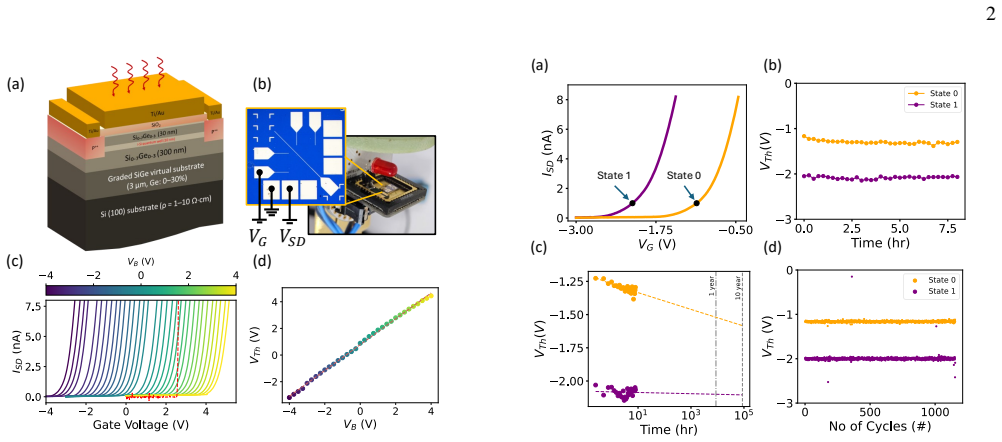
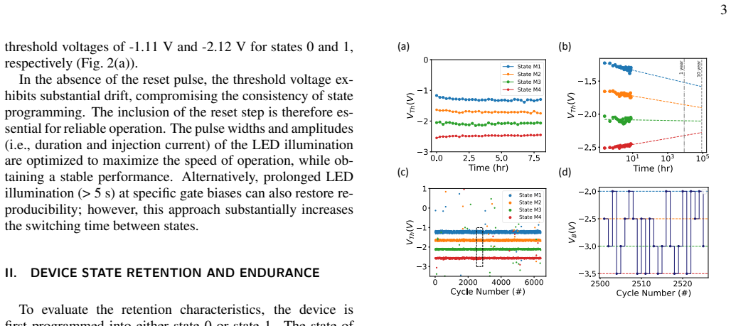
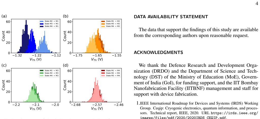
The device exploits a high interface trap density (D_it > 1.6 × 10^12 eV^{-1}cm^{-2}), which, in conjunction with the oxide thickness and dielectric constant, enables effective 'locking' of the threshold voltage to the applied gate bias over a wide voltage range. Two of these states can be selected for binary operation, while the availability of multiple stable states within the same device enables multibit data storage. Robust cycling endurance (>10^3 cycles) and long-term state retention (>10^4 s) of the memory states at 1.5 K confirm the suitability of this approach for integration into Si/SiGe-based quantum computing architectures.
What carries the argument
High interface trap density that locks threshold voltage to gate bias over a voltage range when combined with optical excitation for programming and erasure.
If this is right
- Multiple stable states within one device enable multibit storage without additional hardware.
- Memory states maintain integrity for over 10,000 seconds and survive more than 1,000 cycles at 1.5 K.
- The same Si/SiGe platform supports both the memory and quantum devices, reducing integration complexity.
Where Pith is reading between the lines
- Optical addressing could reduce wiring density in large cryogenic qubit arrays by replacing some electrical control lines.
- The same trap-locking principle might extend to other undoped heterostructures for low-power cryogenic logic.
- Computing-in-memory operations could be tested by performing simple logic directly on the stored states at 1.5 K.
Load-bearing premise
The threshold-voltage locking and optical programmability arise specifically from the measured high interface trap density and remain stable without new degradation under repeated optical cycling at 1.5 K.
What would settle it
Direct measurement of interface trap density before and after cycling that shows either no correlation between trap density and voltage locking or rapid degradation of states after 1000 cycles due to mechanisms unrelated to the reported traps.
Figures
read the original abstract
Scalable cryogenic memory is a critical yet unresolved requirement for large-scale quantum computing architectures, particularly for computing-in-memory schemes. We exploit the interplay between optical excitation and gate bias in an undoped Si/SiGe heterojunction field-effect transistor (HFET) to realize non-volatile memory functionality. The device exploits a high interface trap density ($D_{it} > 1.6 \times 10^{12}$~eV$^{-1}$cm$^{-2}$), which, in conjunction with the oxide thickness and dielectric constant, enables effective "locking" of the threshold voltage to the applied gate bias over a wide voltage range. Two of these states can be selected for binary operation, while the availability of multiple stable states within the same device enables multibit data storage. Robust cycling endurance ($>~10^3$ cycles) and long-term state retention ($>~10^4$~s) of the memory states at 1.5 K confirm the suitability of this approach for integration into Si/SiGe-based quantum computing architectures.
Editorial analysis
A structured set of objections, weighed in public.
Referee Report
Summary. The manuscript claims to realize non-volatile cryogenic flash memory in an undoped Si/SiGe HFET by exploiting optical excitation together with gate bias. A high interface trap density (D_it > 1.6 × 10^12 eV^{-1}cm^{-2}) is asserted to produce stable threshold-voltage locking over a wide bias range, enabling binary and multibit storage; the device is reported to show endurance >10^3 cycles and retention >10^4 s at 1.5 K, making it suitable for Si/SiGe quantum-computing architectures.
Significance. If the mechanism and performance metrics are substantiated, the result would address a recognized gap in scalable cryogenic memory for quantum processors by providing an optically programmable, Si-compatible non-volatile element that operates at millikelvin temperatures without requiring additional doping or complex fabrication.
major comments (2)
- [Abstract] Abstract: The central design rationale attributes V_t locking and optical programmability to the quoted D_it value together with oxide parameters, yet no C-V, conductance, charge-pumping, or temperature-dependent data are supplied to establish this D_it at 1.5 K or to exclude dominant contributions from oxide bulk traps, border traps, or photo-induced carriers. Without such isolation, the claimed mechanism and the assertion of multibit stability under repeated optical cycling remain unverified.
- [Abstract] Abstract: Endurance (>10^3 cycles) and retention (>10^4 s) figures are stated without accompanying measurement protocols, raw traces, error bars, or control-device results that would demonstrate stability against optical-cycling-induced degradation at 1.5 K. These numbers are load-bearing for the suitability claim but cannot be assessed from the provided information.
Simulated Author's Rebuttal
We thank the referee for the constructive comments on our manuscript. We address each major comment below and indicate the revisions that will be incorporated.
read point-by-point responses
-
Referee: [Abstract] Abstract: The central design rationale attributes V_t locking and optical programmability to the quoted D_it value together with oxide parameters, yet no C-V, conductance, charge-pumping, or temperature-dependent data are supplied to establish this D_it at 1.5 K or to exclude dominant contributions from oxide bulk traps, border traps, or photo-induced carriers. Without such isolation, the claimed mechanism and the assertion of multibit stability under repeated optical cycling remain unverified.
Authors: The quoted D_it lower bound was inferred from the observed range of stable threshold-voltage locking combined with the known oxide thickness and dielectric constant. We acknowledge that direct supporting measurements are not presented in the current manuscript. In the revised version we will add C-V and temperature-dependent data acquired at 1.5 K, together with a discussion of how interface-trap versus bulk/border-trap contributions can be distinguished, thereby substantiating the mechanism and the multibit stability claim. revision: yes
-
Referee: [Abstract] Abstract: Endurance (>10^3 cycles) and retention (>10^4 s) figures are stated without accompanying measurement protocols, raw traces, error bars, or control-device results that would demonstrate stability against optical-cycling-induced degradation at 1.5 K. These numbers are load-bearing for the suitability claim but cannot be assessed from the provided information.
Authors: We agree that the endurance and retention metrics require fuller documentation. The revised manuscript will include the detailed measurement protocols, representative raw traces with error bars, and control-device data that confirm stability against optical-cycling degradation at 1.5 K. revision: yes
Circularity Check
No circularity: experimental device results only
full rationale
The paper reports measured device behavior, D_it values, endurance (>10^3 cycles), and retention (>10^4 s) at 1.5 K with no equations, models, or derivations. Claims rest on direct experimental observations of V_t locking and optical programmability rather than any self-referential fitting, prediction, or self-citation chain. No load-bearing steps reduce to inputs by construction.
Axiom & Free-Parameter Ledger
axioms (1)
- domain assumption Standard semiconductor interface physics and dielectric response remain valid at 1.5 K for the Si/SiGe/oxide stack.
Reference graph
Works this paper leans on
-
[1]
These limi- tations highlight the need for new memory concepts that can combine operational stability at low temperatures with scala- bility and integration potential for large-scale cryogenic com- puting systems3. Here, we demonstrate a cryogenic memory concept based on dopant-free Si/SiGe heterojunction field-effect transistors (HFETs) in which the thre...
work page internal anchor Pith review Pith/arXiv arXiv 2026
-
[2]
2.Baptiste A
URLhttps://irds.ieee.org/ images/files/pdf/2020/2020IRDS_CEQIP.pdf. 2.Baptiste A. Cordier, Nicolas P. D. Sawaya, Gian Giacomo Guerreschi, and Shannon K. McWeeney. Biology and medicine in the landscape of quantum advantages.Journal of the Royal Society Interface, 19(196): 20220541,
2020
-
[3]
3.Shamiul Alam, Md Shafayat Hossain, Srivatsa Rangachar Srinivasa, and Ahmedullah Aziz
doi:10.1098/rsif.2022.0541. 3.Shamiul Alam, Md Shafayat Hossain, Srivatsa Rangachar Srinivasa, and Ahmedullah Aziz. Cryogenic memory technologies.Nature Electronics, 6:185–198,
-
[4]
doi:10.1038/s41928-023-00930-2. 4.Swamit S. Tannu, Douglas M. Carmean, and Moinuddin K. Qureshi. Cryogenic-dram based memory system for scalable quantum comput- ers: a feasibility study. InProceedings of the International Sympo- sium on Memory Systems (MEMSYS ’17), pages 189–195. Association for Computing Machinery,
-
[5]
URL https://doi.org/10.1145/3132402.3132436
doi:10.1145/3132402.3132436. URL https://doi.org/10.1145/3132402.3132436. 5.Michael J. Manfra et al. A cryogenic cmos chip for generating control signals for multiple qubits.Nature Electronics, 4:554–564,
-
[6]
doi: https://doi.org/10.1038/s41928-020-00528-y. 6.Chandan Nayak, Joseph C. Wolfe, Alan Bradicich, Xuefeng Wu, Lars Büthe, Nino Samkharadze, Giordano Scappucci, and Floris A. Zwanenburg. Characterizing quantum devices at scale with cus- tom cryo-cmos.Physical Review Applied, 13:054072,
-
[7]
URLhttps://link.aps.org/ doi/10.1103/PhysRevApplied.13.054072
doi: 10.1103/PhysRevApplied.13.054072. URLhttps://link.aps.org/ doi/10.1103/PhysRevApplied.13.054072. 7.Jong-Ho Bae, Jong-Won Back, Min-Woo Kwon, Jae Hwa Seo, Keon Yoo, Sung Yun Woo, Kyungchul Park, Byung-Gook Park, and Jong-Ho Lee. Characterization of a capacitorless dram cell for cryogenic memory ap- plications.IEEE Electron Device Letters, 40(10):1614–1617,
-
[8]
doi: 10.1109/LED.2019.2933504. 8.A. Zaslavsky, C. A. Richter, P. R. Shrestha, B. D. Hoskins, S. T. Le, A. Madhavan, and J. J. McClelland. Impact ionization-induced bistabil- ity in cmos transistors at cryogenic temperatures for capacitorless mem- ory applications.Applied Physics Letters, 119(4):043501, 07
-
[9]
ISSN 0003-6951. doi:10.1063/5.0060343. URLhttps://doi.org/ 10.1063/5.0060343. 9.Yi Han, Jingxuan Sun, Benjamin Richstein, Andreas Grenmyr, Jin- Hee Bae, Frederic Allibert, Ionut Radu, Detlev Grützmacher, Joachim Knoch, and Qing-Tai Zhao. An energy efficient memory cell for quantum and neuromorphic computing at low temperatures.Nano Letters, 25(16):6374–6381, Apr
-
[10]
doi: 10.1021/acs.nanolett.4c05855
ISSN 1530-6984. doi: 10.1021/acs.nanolett.4c05855. URLhttps://doi.org/10.1021/ acs.nanolett.4c05855. 10.A. Grill, E. Bury, J. Michl, S. Tyaginov, D. Linten, T. Grasser, B. Par- vais, B. Kaczer, M. Waltl, and I. Radu. Reliability and variability of advanced cmos devices at cryogenic temperatures. In2020 IEEE Inter- national Reliability Physics Symposium (I...
-
[11]
doi: 10.1109/IRPS45951.2020.9128316. 11.Valery V . Ryazanov, Vitaly V . Bol’ginov, Danila S. Sobanin, Igor V . Vernik, Sergey K. Tolpygo, Alan M. Kadin, and Oleg A. 5 Mukhanov. Magnetic josephson junction technology for digi- tal and memory applications.Physics Procedia, 36:35–41,
-
[12]
doi:https://doi.org/10.1016/j.phpro.2012.06.126
ISSN 1875-3892. doi:https://doi.org/10.1016/j.phpro.2012.06.126. URLhttps://www.sciencedirect.com/science/article/pii/ S1875389212020639. SUPERCONDUCTIVITY CENTENNIAL Con- ference
-
[13]
doi:10.1103/PhysRevApplied.22.034044. URLhttps://doi.org/10. 1103/PhysRevApplied.22.034044. 13.Davide Degli Esposti, Brian Paquelet Wuetz, Viviana Fezzi, Mario Lo- dari, Amir Sammak, and Giordano Scappucci. Wafer-scale low-disorder 2deg in 28Si/sige without an epitaxial si cap.Applied Physics Letters, 120 (18):184003,
-
[14]
URLhttps://doi.org/ 10.1063/5.0088576
doi:10.1063/5.0088576. URLhttps://doi.org/ 10.1063/5.0088576. 14.Yunhui Jang, Yeojin Jeong, Seokjin Jang, Taehyun Cho, Zhong Pan, Jun- zhe Zhang, Yumeng Guo, Kyesoo Kim, Yong-Sang Kim, Sangheon Park, and Junsin Yi. No plasma treatment effects on the structural and electri- cal properties of pecvd-grown sio2 films.ACS Applied Materials & In- terfaces, 17(1...
-
[15]
URL https://doi.org/10.1021/acsami.5c05151
doi:10.1021/acsami.5c05151. URL https://doi.org/10.1021/acsami.5c05151. PMID: 40309894. 15.S. Stathopoulos et al. Multibit memory operation of metal-oxide bi-layer memristors.Scientific Reports, 7:17785,
-
[16]
URLhttps://doi.org/10.1038/s41598-017-17785-1
doi:10.1038/s41598-017- 17785-1. URLhttps://doi.org/10.1038/s41598-017-17785-1. 16.Jae Hur, Dongsuk Kang, Dong Il Moon, Ji Man Yu, Yang Kyu Choi, and Shimeng Yu. Cryogenic storage memory with high-speed, low- power, and long-retention performance.Advanced Electronic Materi- als, 9(6):2201299,
-
[17]
URLhttps: //doi.org/10.1002/aelm.202201299
doi:10.1002/aelm.202201299. URLhttps: //doi.org/10.1002/aelm.202201299. 17.Simon M. Sze and Kwok K. Ng.Physics of Semiconductor De- vices. Wiley, 3 edition,
-
[18]
com/doi/10.1002/9780470068328.ch6
URLhttps://onlinelibrary.wiley. com/doi/10.1002/9780470068328.ch6. See Chapters 6–8 for ox- ide/interface traps, threshold voltage instability, and trap-induced noise. 18.Leonardo Massai, Bence Hetényi, Matthias Mergenthaler, Felix J. Schupp, Lisa Sommer, Stephan Paredes, Stephen W. Bedell, Patrick Harvey-Collard, Gian Salis, Andreas Fuhrer, Nico W. Hendr...
-
[19]
doi:10.1038/s43246-024-00563-8. URLhttps://doi.org/10. 1038/s43246-024-00563-8. 19.J. Yoneda, K. Takeda, T. Otsuka, T. Nakajima, M. R. Delbecq, G. Alli- son, T. Honda, T. Kodera, S. Oda, Y . Hoshi, N. Usami, K. M. Itoh, and S. Tarucha. A quantum-dot spin qubit with coherence limited by charge noise and fidelity higher than 99.9%.Nature Nanotechnology, 13:...
-
[20]
doi:10.1038/s41565-017-0014-x. 20.F. Stampfl, C. Godfrin, S. Kubicek, S. Baudot, B. Raes, K. De Greve, A. Grill, and M. Waltl. C–v characterization of Si/SiGe heterostruc- tures at cryo temperatures. InProceedings of the IEEE Interna- tional Reliability Physics Symposium (IRPS), March
-
[21]
doi: 10.1109/IRPS48204.2025.10982705. 21.Ke Wang, Hai-Ou Li, Gang Luo, Xin Zhang, Fang-Ming Jing, Rui-Zi Hu, Yuan Zhou, He Liu, Gui-Lei Wang, Gang Cao, Hong-Wen Jiang, and Guo-Ping Guo. Improving mobility of silicon metal-oxide-semiconductor devices for quantum dots by high vacuum activation annealing.EPL (Eu- rophysics Letters), 130:27001,
-
[22]
URLhttps://doi.org/10.1209/0295-5075/130/27001
doi:10.1209/0295-5075/130/27001. URLhttps://doi.org/10.1209/0295-5075/130/27001. 22.Nai-Wen Hsu, Wei-Chih Hou, Yen-Yang Chen, Yu-Jui Wu, Hsiang-Shun Kao, Charles Thomas Harris, Tzu-Ming Lu, and Jiun-Yun Li. Temper- ature dependence of charge distributions and carrier mobility in an un- doped si/sige heterostructure.IEEE Transactions on Electron Devices, 69(2), 01
-
[23]
ISSN ISSN 0018-9383. doi:10.1109/ted.2021.3138363. URLhttps://www.osti.gov/biblio/1842836
discussion (0)
Sign in with ORCID, Apple, or X to comment. Anyone can read and Pith papers without signing in.