REVIEW 2 major objections 6 minor 18 references
A single scaling law, δε ∝ α/√N, governs strain-map precision in few-pixel electron diffraction, and the cepstral transform reaches 0.09% precision at 1 nm resolution with a 1 pC dose.
Reviewed by Pith at T0; open to challenge. T0 means a machine referee read the full paper against a public rubric. the ladder, T0–T4 →
The cepstral method achieves 0.09% strain precision at 1 nm resolution on a small-pixel-count detector, with precision scaling proportional to convergence angle over the square root of dose.
T0 review reviewed 2026-08-04 challenge →
load-bearing objection Solid, useful experimental evaluation of EWPC strain mapping on small-pixel detectors; the central claim mostly holds, but the precision metric is likely contaminated by sample fringes and needs a cleaner test before the numbers are taken at face value. the 2 major comments →
Cepstral Strain Mapping for Small Pixel-Count Detectors
The pith
A machine-rendered reading of the paper's core claim, the machinery that carries it, and where it could break.
The reading
Core claim
On its own terms, the claim is that strain measurement precision in nanobeam electron diffraction is fundamentally limited by Poisson counting noise and by the convergence angle, not by detector pixel count. The paper validates a cepstral analysis pipeline in which the logarithm of each convergent-beam pattern is Fourier transformed to produce pair-correlation peaks at projected inter-atomic distances; tracking two of those peaks with sub-pixel interpolation yields the full strain tensor. The measured precision follows δε ∝ α/√N in the low-dose regime, plateaus when dynamical diffraction contrast takes over at high dose, and a 0.09% precision at 1 nm resolution is achieved at 1 pC with a 2 m
What carries the argument
The load-bearing object is the Exit Wave Power Cepstral (EWPC) transform: the Fourier transform of the logarithm of the diffraction pattern, which acts as a pair-correlation function whose peaks sit at projected inter-atomic spacings. Because each cepstral peak integrates periodicity from many Bragg disks, few detector pixels and few pixels per disk suffice; what matters is the total dose N collected inside the usable angular range and the convergence semi-angle α, which enter through the two-pixel detection limit δε ∝ α/√N. The paper uses this identity to interpolate precision across experimental conditions and to locate the crossover where dynamical diffraction, rather than shot noise, set
Load-bearing premise
The reported precision numbers treat small regions of the nominally unstrained silicon as strain-free, so the local scatter in the strain map is counted entirely as measurement noise; real thickness fringes, buckling, or residual tilt in those regions would inflate the precision and skew the scaling fits.
What would settle it
Acquire repeated strain maps of the same silicon wedge after deliberate changes in specimen tilt or at locations with and without visible thickness fringes. If the local standard deviation of the strain map changes systematically with thickness or tilt, the scatter is sample-driven, not pure measurement noise. Alternatively, test the predicted √N scaling directly: at a fixed convergence angle in a verified strain-free region, quadrupling the dose should halve the Poisson-noise contribution; failure to do so would falsify the extrapolation.
If this is right
- A 1 pC, 10 ms-per-pixel exposure can already meet the industry's 0.1% precision / 1 nm resolution target, so production-relevant strain maps can be acquired in seconds.
- Because α enters linearly, any gain in dose or in beam parallelism improves precision only at the cost of spatial resolution; the 2 mrad setting is the reported sweet spot for 0.09% at 1 nm.
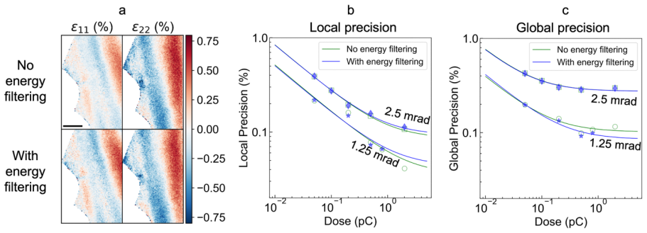
- Precession should be used whenever sample thickness variations or dynamical contrast dominate, improving local precision by 1.3–2× and global precision by 1.5–2.5×.
- Energy filtering can be omitted for device-relevant thicknesses, removing a hardware burden unless the spectrometer itself distorts the diffraction pattern.
- The method works with compact data sets and no tunable fitting parameters, making live processing and high-throughput mapping feasible.
Where Pith is reading between the lines
- If the scaling law holds at lower doses, the same pipeline could be pushed toward low-dose imaging by adding a pre-filter that suppresses diffuse-scattering noise, which the paper itself notes the logarithm can overweight.
- The high-dose plateau implies that for thick or strongly scattering samples, more dose stops helping; the next lever is precession or choosing reflections less affected by dynamical contrast, not simply raising beam current.
- The thickness-fringe artifacts suggest that global precision over a large field of view, not just local precision on a flat region, is the metric that will predict real-device performance; a standard strain-free wedge with documented thickness and tilt would make algorithm comparisons meaningful.
- Detector developments that raise saturation current and frame rate translate directly into better precision at fixed dwell time through the √N factor, giving a quantitative target for next-generation pixel-array detectors.
Editorial analysis
A structured set of objections, weighed in public.
Referee Report
Summary. The paper evaluates the Exit Wave Power Cepstral (EWPC) transform for strain mapping with small-pixel-count 4D-STEM detectors (e.g., EMPAD). It reports precision measurements on nominally unstrained Si and on Si-SiGe multilayers, and claims a measured precision of 0.09% at 1 nm resolution for a 1 pC dose with a 2 mrad convergence semi-angle. The authors propose that precision scales as δε ∝ α/√N, with an additional constant systematic term at high dose, and demonstrate improvements from precession electron diffraction and a lack of strong improvement from zero-loss energy filtering for the studied thicknesses. The manuscript includes code availability and a systematic parameter study, but the central empirical precision values and the scaling law rest on the assumption that the chosen sample regions contain no real strain variations.
Significance. If the reported precision and scaling are correct, the work is significant for high-throughput semiconductor strain metrology: it directly addresses the small-pixel-count limitation of fast pixel-array detectors and offers a practical algorithm with public code. The systematic comparison across dose, convergence angle, thickness, precession, and energy filtering is valuable, and the paper honestly identifies regimes (Poisson-noise-limited vs systematic-error-limited) that are important for practical users. The strength of the paper is its empirical scope and the explicit presentation of the scaling ansatz; however, the headline precision numbers are only as strong as the assumption that the measurement regions are truly strain-free, an issue the paper itself partly exposes in Fig. 5.
major comments (2)
- [Results (Fig. 4 and Fig. 5)] The headline precision values are the local standard deviation of measured strain over a ~10x10-pixel region of a 'nominally unstrained' Si [110] foil. This metric equals measurement noise only if that region contains no real strain variation. The paper itself shows, on the same material, that thickness fringes produce alternating strain bands in EWPC strain maps (Fig. 5b) and that the local precision varies with thickness (Fig. 5c). No evidence is given that the region used for Fig. 4 is free of thickness gradients, residual tilt, buckling, or FIB damage. Any such spatially varying real strain would be absorbed into the fitted a and b parameters, biasing the claimed dose and α scalings. This is load-bearing for the central claim, so the authors should either demonstrate strain-free conditions in the exact measurement regions (e.g., with an independent measure such as a large-angle rocki
- [Eq. (1) and Supplementary Fig. 5] The central scaling δε ∝ α/(θ_B√N) is presented as an analytical result from Chapman et al., but the proportionality constant is left unspecified and the experimental test of the α-dependence is a linear fit of the fitted parameter a versus α. This is a fitted trend, not a parameter-free prediction. The manuscript states the trend is 'roughly' consistent, but no uncertainties, goodness-of-fit values, or numbers of points are reported. Since this scaling is used to interpolate precision across experimental conditions and to justify the trade-off in Fig. 4(b), the fit should be reported with confidence intervals and, ideally, cross-validated against multislice simulations with known strain and dose.
minor comments (6)
- [Scaling of Precision with Numerical Aperture and Dose] Eq. (1) is garbled in the text ('δε∝αθ+91N'); it should be rendered as δε ∝ α/(θ_B√N). Also, the Introduction says 'α√N scaling' where 'α/√N' is meant.
- [Discussion] The Discussion recommends a pre-filtering step for low-dose analysis, but the headline 0.09% precision at 1 pC was obtained without one. Please clarify whether the reported number already benefits from pre-filtering or whether the recommendation post-dates the measurement.
- [Fig. 4(b)] The probe-size values 'account for the finite source size', but the calculation of ds is not described. Since the resolution/precision trade-off is a central figure, a short definition or reference is needed.
- [Supplementary Text 2] The exponential fit to parameter b versus α is presented without justification. If b is intended to represent dynamical-diffraction systematic errors, a physical model or at least a discussion of alternative functional forms would strengthen the interpretation.
- [Methods (peak fitting)] The size of the region around the EWPC peaks is 'manually chosen'. Since this choice can affect the fitted peak positions and hence the precision, the authors should state the actual region size used for Figs. 4-7 and comment on sensitivity.
- [General] The paper lacks a data availability statement for the experimental datasets; only code is provided. For an empirical study of this type, making the representative raw 4D-STEM datasets available would improve reproducibility.
Circularity Check
No significant circularity: central precision scaling is an externally borrowed model tested with free fit parameters; the cepstral method itself is evaluated against new experimental data and external benchmarks.
full rationale
The paper's central scaling law, δε ∝ α/(θ_B√N) (Eq. 1), is explicitly attributed to Chapman et al. (1978), an independent external reference, not to the authors' prior work. The empirical precision values are measured as the standard deviation of strain over small regions of nominally unstrained Si, and the dose–precision data for each convergence angle are fitted to σ = sqrt((a/√N)^2 + b^2) with free parameters a and b. The subsequent plot of a versus α is a genuine falsifiable test of the borrowed scaling: nothing in the fitting procedure forces a to be proportional to α, and the reported behavior could in principle have failed. The cepstral transform methodology is cited to the authors' earlier Padgett et al. (2020) paper, but the present manuscript independently evaluates it on Si wedges, Si–SiGe multilayers, precession, and energy-filtered datasets, and compares against py4DSTEM and a commercial strain-analysis package. This is an experimental evaluation, not a self-referential derivation. Possible contamination of precision metrics by real strain variations, as suggested by the thickness-fringe artifacts in Fig. 5, is a correctness/validity concern that the paper itself partially acknowledges, but it is not a circularity because the precision estimates are measurements rather than quantities defined by the model being tested. No equation is shown to be equivalent to its own input by construction, and no load-bearing argument reduces to an unverified self-citation.
Axiom & Free-Parameter Ledger
free parameters (2)
- a (Poisson-noise coefficient) =
varies with α (fit parameter in Fig. 4a; plotted in Supp. Fig. 5)
- b (systematic-error offset) =
varies with α (fit parameter in Fig. 4a; plotted in Supp. Fig. 5)
axioms (3)
- domain assumption The minimum detectable shift of a constant-intensity disk on a two-pixel detector is θ = ... (Chapman et al. 1978), from which δε ∝ α/√N is asserted to apply to EWPC peak tracking.
- domain assumption The sample regions used to measure precision are free of real strain variations, so the local standard deviation reflects measurement noise.
- standard math The cepstral peaks are bandwidth-limited, so Whittaker-Shannon interpolation yields unbiased sub-pixel maxima.
Cite this review
Pith. "Pith review of Cepstral Strain Mapping for Small Pixel-Count Detectors." pith.science (2026). https://pith.science/paper/HLUYKOQE
@misc{pith2026250908321,
  author       = {Pith},
  title        = {Pith review of: Cepstral Strain Mapping for Small Pixel-Count Detectors},
  year         = {2026},
  howpublished = {\url{https://pith.science/paper/HLUYKOQE}},
  note         = {Machine review of arXiv:2509.08321}
}
read the original abstract
With the decreasing sizes of integrated-circuit components, the semiconductor industry is in growing need of high-throughput strain mapping techniques that offer high precision and spatial resolution, with desired industry goals of 0.01-0.1% and 1 nm respectively. As the fundamental limitation on the measurement precision is set by the Poisson noise, pixel array detectors with high saturation current, high dynamic range and fast readout are ideally suited for this purpose. However, due to the limited pixel count on these detectors, they do not work well with traditional strain mapping algorithms that were optimized to work on datasets with a large pixel count. Here, we evaluate the cepstral transform that was designed to address this problem, with the precision determined by the convergence, collection angles and dose while remaining insensitive to the pixel count. We test the performance of our method on silicon wedges and Si-SiGe multilayers, and using datasets collected at different conditions, we show how the measured strain precision scales as a function of dose, aperture size and sample thickness. Using precession gives a further improvement in precision by about 1.5-2x, whereas energy filtering does not have a significant impact on the cepstral method for device-relevant sample thickness ranges.
Figures


Reference graph
Works this paper leans on
-
[1]
1 Cepstral Strain Mapping for Small Pixel-Count Detectors Harikrishnan KP1,*, Dasol Yoon1,2, Yu-Tsun Shao1,3, Zhaslan Baraissov1, Luigi Mele4, Christoph Mitterbauer4, Erik Kieft4, Stefano Vespucci4, David A. Muller1,5,* 1School of Applied and Engineering Physics, Cornell University, Ithaca, NY, USA 2Department of Materials Science and Engineering, Cornell...
work page 2016
-
[5]
and edge-detection (Müller et al., 2012; Yuan et al.,
work page 2012
-
[6]
Influence of precession on strain mapping. (a) Direct comparison of strain maps calculated from datasets taken with and without precession at the same experimental conditions (dose = 2 pC, α = 2.5 mrad). Plots comparing the change in (b) local precision and (c) global precision when precession is used. Solid blue markers and hollow green markers represent...
work page 2012
-
[9]
that can reduce dynamical diffraction artifacts. Our preliminary strain mapping results on silicon wedge samples with EWPC were reported in 5 conference proceedings (Harikrishnan et al., 2021; Yoon et al., 2022). We extend these here, including to a SiGe multilayer. Materials and Methods Experiments and Simulation The samples used in the study were prepar...
work page 2021
-
[12]
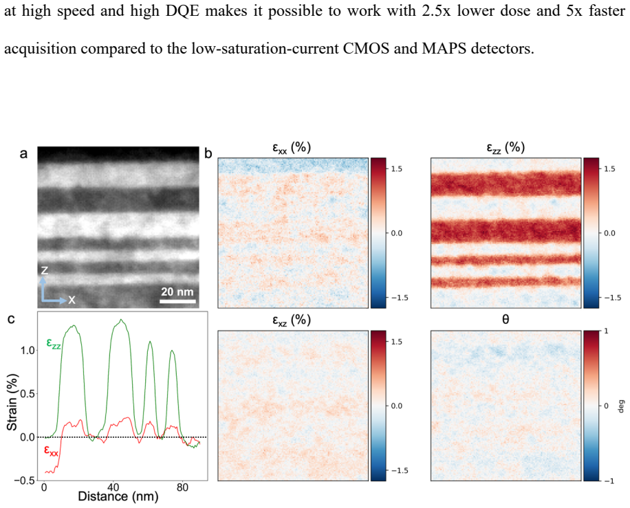
While increased dose leads to a slight improvement in precision as evident from the smoother strain maps, the persistence of strain features in the εxx map indicate that they stem from differences in dynamical diffraction between the two layers from the unavoidable thin-film relaxation coupled with a slight mistilt (Hÿtch & Minor, 2014). Although cross-co...
work page 2014
-
[14]
zone axis, which could be good standard samples for such tests due to its universal use in semiconductor devices, also making it directly relevant to industry applications. Code Availability Both the MATLAB and Python versions of the code for cepstral analysis are made freely available and can be accessed at the following links: MATLAB - https://github.co...
work page 2015
-
[16]
OPHUS, C. (2019). Four-Dimensional Scanning Transmission Electron Microscopy (4D-STEM): From Scanning Nanodiffraction to Ptychography and Beyond. Microscopy and Microanalysis 563–582. PADGETT, E., HOLTZ, M. E., CUEVA, P., SHAO, Y. T., LANGENBERG, E., SCHLOM, D. G. & MULLER, D. A. (2020). The exit-wave power-cepstrum transform for scanning nanobeam electro...
work page internal anchor Pith review Pith/arXiv arXiv 2019
-
[110]
zone axis to test the performance of the EWPC algorithm on 4D-STEM datasets taken on the EMPAD-G2 detector. We track the positions of the closest EWPC peaks in the (111) and (111) directions and use their symmetric and anti-symmetric linear combinations as the basis vectors for the strain tensor in two dimensions. A virtual annular dark field (ADF) image ...
work page 1984
-
[209]
Patterned Probes for High Precision 4D-STEM Bragg Measurements
http://arxiv.org/abs/1907.05504. ZHANG, X., PADGETT, E., ZHU, L., BUHRMAN, R. & MULLER, D. (2020). A Robust Basis for Grain Identification in Polycrystalline Thin Film Devices Using Cepstrum Transforms of 4D-STEM Diffraction Pattern. Microscopy and Microanalysis 26, 1620–1622. ZUO, J. M. & MABON, J. C. (2004). Web-Based Electron Microscopy Application Sof...
work page internal anchor Pith review Pith/arXiv arXiv 1907
-
[231]
G., MEFFERT, M., HOERMANN, C., ZAMBON, P., BACHEVSKAYA, D., REMIGY, H., SCHULZE-BRIESE, C
STROPPA, D. G., MEFFERT, M., HOERMANN, C., ZAMBON, P., BACHEVSKAYA, D., REMIGY, H., SCHULZE-BRIESE, C. & PIAZZA, L. (2023). From STEM to 4D STEM: Ultrafast Diffraction Mapping with a Hybrid-Pixel Detector. Microscopy Today 31, 10–14. SUN, Z., BARAISSOV, Z., PORTER, R. D., SHPANI, L., SHAO, Y.-T., OSEROFF, T., THOMPSON, M. O., MULLER, D. A. & LIEPE, M. U. ...
work page 2023
-
[1963]
where it is widely used for deconvolving a slowly-varying envelope function from the carrier wave and has broad applications in autotuning and speech analysis. A direct cepstral transform would start with what in electron microscopy would be the ideal real-space exit wave and then calculating the power spectrum, a step that is accomplished in EWPC by form...
work page 2020
-
[2010]
The Bloch wave simulations were done using the EMAPS package (Zuo & Mabon, 2004)
in MuSTEM. The Bloch wave simulations were done using the EMAPS package (Zuo & Mabon, 2004). Strain mapping using the EWPC transform The exit wave power cepstrum (EWPC) is a non-linear transformation applied on diffraction patterns that results in a real-space representation of the distances in the crystal structure being probed (Padgett et al., 2020). It...
work page 2004
-
[2019]
are designed to work on diffraction data collected with a large pixel-count detector. However, precise tracking of diffraction disk shifts for strain mapping does not fundamentally depend on a large pixel count. Numerical simulations of center-of-mass calculations have shown that the precision of disk detection improves with increasing pixel count only up...
work page 2018
-
[2020]
was developed to meet these demands, with its performance determined by the maximum dose, and the largest usable angle, rather than the number of detector pixels. In addition to strain mapping applications (Padgett et al., 2023; Kavle et al., 2024), the cepstral transform has also been used for the imaging of lattice distortions using the diffuse scatteri...
work page 2023
-
[2021]
and other 4D-STEM techniques (Ophus, 2019). However, their limited pixel count (128 x 128 for EMPADs and 192 x 192 or 96 x 96 for ARINA) presents a challenge for strain mapping applications, as common strain mapping algorithms like template cross-correlation (Müller et al., 2012; Pekin et al., 2017; Zeltmann et al., 2020; Savitzky et al.,
work page 2019
-
[2022]
and DECTRIS ARINA (Zambon et al., 2023; Stroppa et al.,
work page 2023
-
[2023]
are gaining widespread adoption for high speed and high current diffraction measurements required for ptychography (Nellist et al., 1995; Jiang et al., 2018; Chen et al.,
work page 1995
-
[7766]
GIBSON, J. M., HULL, R., BEAN, J. C. & TREACY, M. M. J. (1985). Elastic relaxation in transmission electron microscopy of strained‐layer superlattices. Applied Physics Letters 46, 649–651. GIBSON, J. M. & TREACY, M. M. J. (1984). The effect of elastic relaxation on the local structure of lattice-modulated thin films. Ultramicroscopy 14, 345–349. 26 HÄHNEL...
work page 1985
This paper was first reviewed by deepseek-v4-flash on August 4, 2026.
discussion (0)
Sign in with ORCID, Apple, or X to comment. Anyone can read and Pith papers without signing in.