REVIEW 2 major objections 5 minor 48 references
Resonance shifts in NbTiN spiral inductors under heat and field are mostly inductive, and geometry sets both temperature sensitivity and field robustness for qubit readout.
Reviewed by Pith at T0; open to challenge. T0 means a machine referee read the full paper against a public rubric. the ladder, T0–T4 →
T0 review · grok-4.5
2026-07-12 09:41 UTC pith:Y3Y4LRAC
load-bearing objection Solid dual-method characterization of NbTiN spirals under warmer, near-tesla conditions; useful design metrics, ordinary experimental caveats. the 2 major comments →
Superconducting Spiral Inductors for RF Reflectometry: Operation at Elevated Temperatures and Magnetic Fields
The pith
A machine-rendered reading of the paper's core claim, the machinery that carries it, and where it could break.
Core claim
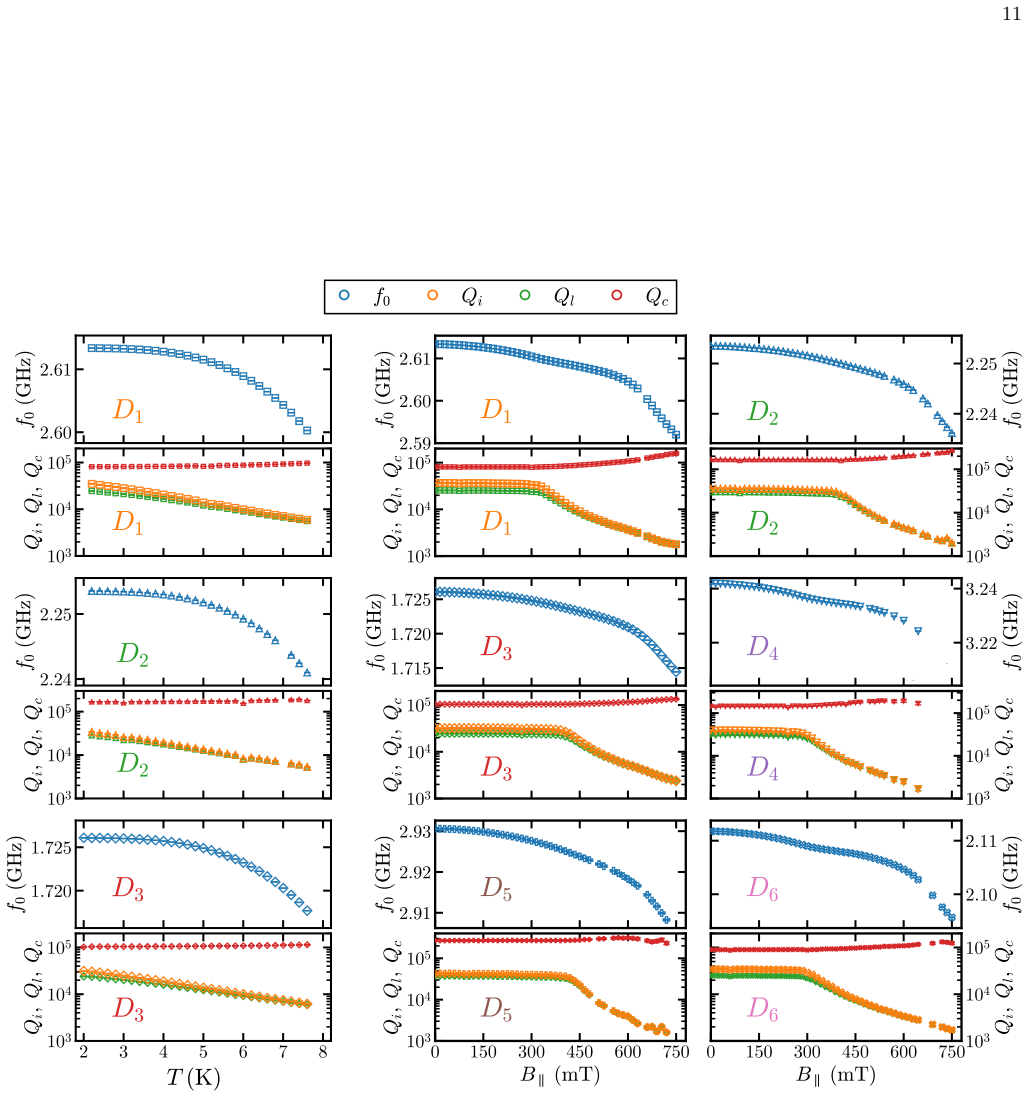
Temperature- and magnetic-field-dependent resonance shifts of NbTiN spiral inductors are predominantly inductive in origin. They can be reconstructed from independently measured inductance L(T,B) using one fixed self-capacitance C_self. The same data yield practical design metrics: the kinetic-inductance fraction α = L_k/(L_g + L_k) that sets temperature sensitivity of f0, and a field-degradation scale B_Q that falls with track width and marks the onset of vortex-related quality-factor loss under residual perpendicular field.
What carries the argument
Dual-measurement reconstruction: weakly coupled notch resonators give f0 and Qi, while low-frequency two-port admittance fits give L independently; a single geometry-fixed C_self then rebuilds f0 via f0 = 1/(2π√(L C_self)), isolating inductive origin of the shifts and enabling α and B_Q design metrics.
Load-bearing premise
Self-capacitance is assumed fixed by geometry alone and unchanged by temperature or magnetic field, so any frequency shift can be blamed entirely on inductance.
What would settle it
Repeat the two-port L and notch f0 runs on the same device under deliberately pure in-plane field (misalignment ≪ 0.5°) and check whether the fixed-C_self reconstruction still matches f0(B) within uncertainty, or whether residual f0 disagreement and the B_Q drop vanish when the perpendicular component is removed.
Editorial analysis
A structured set of objections, weighed in public.
Referee Report
Summary. The manuscript reports a systematic experimental study of NbTiN spiral inductors intended for RF-reflectometry readout of semiconductor spin qubits, under temperatures of several kelvin and in-plane magnetic fields approaching 1 T. Using two complementary microwave setups—weakly coupled notch resonators (set-up 1) and two-port admittance-matrix inductance extraction (set-up 2)—the authors separate inductive and capacitive contributions. They show that temperature- and field-dependent resonance-frequency shifts are predominantly inductive, reconstructible from independently measured L(T,B) with a single fixed C_self via Eq. (2). Quality-factor degradation is attributed to quasiparticle loss (Eq. 5) and residual-perpendicular-field vortex entry (B_Q). Practical design metrics α = L_k/(L_g + L_k) and B_Q(w) are introduced to link geometry to temperature sensitivity and field robustness.
Significance. If the dual-setup reconstruction holds, the work supplies a concrete, transferable benchmarking framework for superconducting spiral inductors under the elevated-T and finite-B conditions increasingly targeted for scalable spin-qubit architectures. Strengths include independent validation of the inductance extraction against a commercial Coilcraft 100 nH part (Appendix E), consistency of microwave-fitted T_c with DC resistance (Appendix F), quantitative error estimates from circle-fit covariances and bond-wire corrections, and explicit geometry–performance metrics (α, B_Q) that can guide future design trade-offs between footprint, frequency stability and field resilience. The intermediate kinetic-inductance regime of the NbTiN spirals is usefully positioned relative to both surface-mount inductors and more aggressive superinductor approaches.
major comments (2)
- Sec. III and Fig. 3(b): the field reconstruction of f0(B∥) from measured L(B∥) plus fixed C_self = 44 fF shows a visibly larger residual mismatch than the temperature case. The text attributes this solely to run-to-run misalignment (θ ∼ 5°). Because the inductive-origin claim for magnetic field rests on this reconstruction, a quantitative bound on residual Bz (or a co-mounted Hall sensor / simultaneous L and f0 measurement on the same cool-down) would strengthen the central claim that capacitive contributions remain negligible under field.
- Sec. IV–V and Appendix G: B_Q is defined operationally as the 10 % drop in Qi and is then fitted to a phenomenological vortex-entry model (Eq. G1) that introduces free parameters θ_j and C. While the observed B_Q ∝ 1/w trend is clear, the manuscript should state more explicitly that B_Q is a practical figure of merit under residual misalignment rather than an intrinsic material critical field; otherwise the design metric risks being over-interpreted as geometry-independent.
minor comments (5)
- Table I: several L_meas entries are blank (“–”); a short note explaining why only a subset of devices received two-port extraction would improve transparency.
- Fig. 3 caption and Sec. III: the two D2 devices used for L(T) and f0(T) are “nominally identical” but physically distinct; a quantitative statement of device-to-device variation (or a single-device dual-setup measurement) would further support the C_self-constancy claim.
- Eq. (5) and Fig. 4(b): the quasiparticle model is fitted with essentially one free parameter A; reporting the reduced-χ² or residual variance would help the reader judge the quality of the high-T description.
- Appendix D: the ±20 % bond-wire inductance uncertainty is stated but not propagated into the error bars of Fig. 3; adding this would make the L(T,B) uncertainties more complete.
- Typographical: “Deviced out n w gLength” header in Table I appears truncated; “UOSM” is introduced without expansion on first use in the main text (only later as Unknown-Thru-Open-Short-Match).
Circularity Check
No significant circularity: dual independent measurements of L and f0 provide a genuine consistency test that C_self is constant, not a by-construction identity.
full rationale
The paper's central claim (temperature- and field-dependent resonance shifts are predominantly inductive and reconstructible from independently measured L with fixed C_self) rests on two complementary experimental configurations performed on nominally identical devices: set-up 1 (weakly coupled notch resonators yielding f0 and Qi) and set-up 2 (two-port admittance-matrix extraction of L). C_self is obtained once from the 2 K values of L and f0 via Eq. 2 and then held fixed; the subsequent reconstruction of f0(T) and f0(B) from the measured L(T,B) is therefore a non-trivial consistency check. Agreement would fail if C_self varied appreciably with T or B or if the two setups were inconsistent. The BCS fit for Lk,□(T) and the quasiparticle model for Qi(T) introduce free parameters (Lk,□, Δ0, A, Qother) that are used only to interpret the data, not to define the measured shifts. Design metrics α = Lk/(Lg + Lk) and BQ(w) are likewise extracted quantities correlated against independently measured fractional frequency shifts and quality-factor onsets; they are not predictions forced by the same fit. No self-citation is load-bearing for uniqueness, no ansatz is smuggled in via prior work of the authors, and no known empirical pattern is merely renamed. The derivation chain is therefore self-contained experimental validation, not circular.
Axiom & Free-Parameter Ledger
free parameters (6)
- sheet kinetic inductance Lk,□(0) =
1.74 pH/sq
- zero-temperature gap Δ0 and Tc from microwave L(T) fit =
Δ0=2.2 meV, Tc=13.4 K
- quasiparticle prefactor A and Q_other in Eq. 5 =
Q_other=2.8e4; A free
- effective field misalignment angles θ and offset C in vortex model Eq. G1 =
θ~5°, Δθ~0.5°
- B_Q definition threshold =
10% Qi drop
- bond-wire inductance correction =
~4±1 nH typical
axioms (6)
- domain assumption BCS temperature dependence of the superconducting gap enters Lk,□(T) via Eq. 4.
- domain assumption Modified Wheeler formula gives geometric spiral inductance Lg from layout (Appendix A).
- ad hoc to paper Self-capacitance C_self is set by geometry and is independent of T and B over the measured range.
- domain assumption Qi degradation above B_Q is dominated by vortex-associated microwave loss from residual perpendicular field.
- domain assumption Low-frequency two-port response is a lumped series R–L with fixture shunt Cg, not spiral C_self.
- domain assumption At ~−50 dBm, TLS loss is largely saturated so T/B trends reflect the superconducting film.
invented entities (1)
-
B_Q field-degradation scale (10% Qi drop)
no independent evidence
read the original abstract
Superconducting spiral inductors are emerging as key components for radio-frequency (RF) reflectometry, a widely used readout technique for semiconductor spin qubits. Future scalable quantum-computing architectures are expected to operate at elevated temperatures and magnetic fields, placing new demands on the performance and stability of superconducting circuit elements. Here, we present a systematic study of NbTiN spiral inductors under temperatures of several kelvin and magnetic fields approaching 1 T. By combining weakly coupled resonator measurements with independent two-port inductance extraction, we separate inductive and capacitive contributions to device behaviour and directly identify the origin of resonance shifts and quality factor degradation. Furthermore, we establish practical design metrics linking geometry, temperature sensitivity, and magnetic-field robustness. These results provide a general framework for benchmarking superconducting inductors and guiding the design of future RF-reflectometry circuits for practical quantum technologies.
Figures


Reference graph
Works this paper leans on
-
[1]
(e) Equivalent circuit diagram for measurements carried out with set-up 2
(d) ExperimentalS 21 notch response as a function of fre- quency for deviceD 3 at 2 K (red dot) and circle fits (black dashed). (e) Equivalent circuit diagram for measurements carried out with set-up 2. (f) Schematic representation of a spiral wire-bonded to a CPW for 2-port inductance extrac- tion. (g)S-parameter experimental response (dot) and fit (dash...
-
[2]
R. J. Schoelkopf, P. Wahlgren, A. A. Kozhevnikov, P. Delsing, and D. E. Prober, The radio-frequency single- electron transistor (RF-SET): A fast and ultrasensitive electrometer, Science280, 1238 (1998)
1998
-
[3]
Ahmed, J
I. Ahmed, J. A. Haigh, S. Schaal, S. Barraud, Y. Zhu, C.- M. Lee, M. Amado, J. W. A. Robinson, A. Rossi, J. J. L. Morton, and M. F. Gonzalez-Zalba, Radio-frequency ca- pacitive gate-based sensing, Physical Review Applied10, 014018 (2018)
2018
-
[4]
Vigneau, F
F. Vigneau, F. Fedele, A. Chatterjee, D. Reilly, F. Kuem- meth, M. F. Gonzalez-Zalba, E. A. Laird, and N. Ares, Probing quantum devices with radio-frequency reflectom- etry, Applied Physics Reviews10, 021305 (2023)
2023
-
[5]
S. Bugu, S. Nishiyama, K. Kato, Y. Liu, S. Murakami, T. Mori, T. Ferrus, and T. Kodera, 4.2 K sensitivity- tunable radio frequency reflectometry of a physically de- fined p-channel silicon quantum dot, Scientific Reports 11, 20039 (2021)
2021
-
[6]
A. O. Denisov, G. Fuchs, S. W. Oh, and J. R. Petta, Dispersive readout of a silicon quantum device using an atomic force microscope-based RF gate sensor, Applied Physics Letters123, 093502 (2023)
2023
-
[7]
Beilvert, N
C. Beilvert, N. Vivien, C. Thomas, J. Charbonnier, E. Deschaseaux, F. Badets, and J.-P. Michel, Broadband RF characterization and modeling of superconducting coplanar waveguides, IEEE Transactions on Applied Su- perconductivity35, 1 (2024)
2024
-
[8]
A. J. Annunziata, D. F. Santavicca, L. Frunzio, G. Cate- lani, M. J. Rooks, A. Frydman, and D. E. Prober, Tunable superconducting nanoinductors, Nanotechnol- ogy21, 445202 (2010)
2010
-
[9]
Maleeva, L
N. Maleeva, L. Gr¨ unhaupt, T. Klein, F. L´ evy-Bertrand, O. Dupr´ e, M. Calvo, F. Valenti, P. Winkel, F. Friedrich, W. Wernsdorfer, A. V. Ustinov, H. Rotzinger, A. Mon- fardini, M. V. Fistul, and I. M. Pop, Circuit quantum electrodynamics of granular aluminum resonators, Na- ture Communications9, 3889 (2018)
2018
-
[10]
T. H. Swift, F. Olivieri, G. Aizpurua-Iraola, J. Kirk- man, G. M. Noah, M. de Kruijf, F. E. von Horstig, A. Gomez-Saiz, J. J. L. Morton, and M. F. Gonzalez- Zalba, A superinductor in a deep sub-micron in- tegrated circuit, arXiv preprint arXiv:2507.13202 10.48550/arXiv.2507.13202 (2025), arXiv:2507.13202 [quant-ph]
-
[11]
J. I. Colless, A. C. Mahoney, J. M. Hornibrook, A. C. Do- herty, H. Lu, A. C. Gossard, and D. J. Reilly, Dispersive readout of a few-electron double quantum dot with fast RF gate sensors, Phys. Rev. Lett.110, 046805 (2013)
2013
-
[12]
C. H. Yang, R. C. C. Leon, J. C. C. Hwang, A. Saraiva, T. Tanttu, W. Huang, J. C. Lemyre, K. W. Chan, K. Y. Tan, F. E. Hudson, K. M. Itoh, A. Morello, M. Pioro- Ladri` ere, A. Laucht, and A. S. Dzurak, Operation of a silicon quantum processor unit cell above one kelvin, Na- ture580, 350 (2020)
2020
-
[13]
P. Hamonic, M. Toubeix, G. Haas, J. Nath, M. C. Dartiailh, B. Martinez, B. Bertrand, H. Niebojewski, M. Vinet, C. B¨ auerle, F. Balestro, T. Meunier, and M. Urdampilleta, Single-shot in situ readout of a spin qubit unit cell, Nature Electronics 10.1038/s41928-026- 01654-9 (2026)
-
[14]
L. C. Camenzind, S. Geyer, A. Fuhrer, R. J. Warbur- ton, D. M. Zumb¨ uhl, and A. V. Kuhlmann, A hole spin qubit in a fin field-effect transistor above 4 kelvin, Nature Electronics5, 178 (2022)
2022
-
[15]
M. F. Gonzalez-Zalba, S. de Franceschi, E. Charbon, T. Meunier, M. Vinet, and A. S. Dzurak, Scaling silicon- based quantum computing using CMOS technology, Na- ture Electronics4, 872 (2021)
2021
-
[16]
Ferrero and U
A. Ferrero and U. Pisani, Two-port network analyzer cal- ibration using an unknown ‘thru’, IEEE Microwave and Guided Wave Letters2, 505 (1992)
1992
-
[17]
Peruzzo, A
M. Peruzzo, A. Trioni, F. Hassani, M. Zemlicka, and J. M. Fink, Surpassing the resistance quantum with a geometric superinductor, Physical Review Applied14, 044055 (2020)
2020
-
[18]
Probst, F
S. Probst, F. B. Song, P. A. Bushev, A. V. Ustinov, and M. Weides, Efficient and robust analysis of complex scat- tering data under noise in microwave resonators, Review of Scientific Instruments86, 024706 (2015)
2015
-
[19]
D. M. Pozar,Microwave Engineering, 4th ed. (Wiley, 2011)
2011
-
[20]
Tinkham,Introduction to Superconductivity, 2nd ed
M. Tinkham,Introduction to Superconductivity, 2nd ed. (Dover Publications, Mineola, NY, 2004)
2004
-
[21]
C. Song, T. W. Heitmann, M. P. DeFeo, K. Yu, R. Mc- Dermott, M. Neeley, J. M. Martinis, and B. L. T. Plourde, Microwave response of vortices in superconduct- ing thin films of Re and Al, Physical Review B79, 174512 (2009)
2009
-
[22]
S. Kwon, A. F. Roudsari, O. W. B. Benningshof, Y.-C. Tang, H. R. Mohebbi, I. A. J. Taminiau, D. Langenberg, S. Lee, G. Nichols, D. G. Cory, and G.-X. Miao, Magnetic field dependent microwave losses in superconducting nio- bium microstrip resonators, Journal of Applied Physics 124, 033903 (2018)
2018
-
[23]
C. W. Zollitsch, J. O’Sullivan, O. W. Kennedy, G. Dold, and J. J. L. Morton, Tuning high-Q superconducting res- onators by magnetic field reorientation, AIP Advances9, 125225 (2019)
2019
-
[24]
C. R. H. McRae, H. Wang, J. Gao, M. R. Vissers, T. Brecht, A. Dunsworth, D. P. Pappas, and J. Mutus, Materials loss measurements using superconducting mi- crowave resonators, Review of Scientific Instruments91, 091101 (2020)
2020
-
[25]
D. C. Mattis and J. Bardeen, Theory of the anomalous skin effect in normal and superconducting metals, Phys- ical Review111, 412 (1958)
1958
-
[26]
Gao,The Physics of Superconducting Microwave Res- onators, Ph.D
J. Gao,The Physics of Superconducting Microwave Res- onators, Ph.D. thesis, California Institute of Technology (2008)
2008
-
[27]
Zmuidzinas, Superconducting microresonators: Physics and applications, Annual Review of Condensed Matter Physics3, 169 (2012)
J. Zmuidzinas, Superconducting microresonators: Physics and applications, Annual Review of Condensed Matter Physics3, 169 (2012)
2012
-
[28]
P. J. de Visser, J. J. A. Baselmans, P. Diener, S. J. C. Yates, A. Endo, and T. M. Klapwijk, Number fluctua- tions of sparse quasiparticles in a superconductor, Phys- ical Review Letters106, 167004 (2011)
2011
-
[29]
A. P. Zhuravel, C. Kurter, A. V. Ustinov, and S. M. An- lage, Unconventional rf photoresponse from a supercon- ducting spiral resonator, arXiv preprint arXiv:1203.3998 (2012), arXiv:1203.3998. 13
Pith/arXiv arXiv 2012
-
[30]
B. G. Ghamsari, J. Abrahams, S. Remillard, and S. M. Anlage, High-temperature superconducting spiral res- onator for metamaterial applications, arXiv preprint arXiv:1210.4080 (2012), arXiv:1210.4080
Pith/arXiv arXiv 2012
-
[31]
Medahinne, Y
M. Medahinne, Y. P. Kandel, S. Thapa Magar, E. Cham- pion, J. M. Nichol, and M. S. Blok, Magnetic-field- tolerant superconducting spiral resonators for circuit qed, Physical Review Applied23, 014070 (2025)
2025
-
[32]
J. Gao, M. Daal, J. M. Martinis, A. Vayonakis, J. Zmuidzinas, B. Sadoulet, B. A. Mazin, P. K. Day, and H. G. Leduc, Experimental study of the kinetic induc- tance fraction of superconducting coplanar waveguide, Nuclear Instruments and Methods in Physics Research Section A: Accelerators, Spectrometers, Detectors and Associated Equipment559, 585 (2006)
2006
-
[33]
T. M. Bretz-Sullivan, R. M. Lewis, A. L. Lima-Sharma, D. Lidsky, C. M. Smyth, C. T. Harris, M. Venuti, S. Eley, and T.-M. Lu, High kinetic inductance NbTiN supercon- ducting transmission line resonators in the very thin film limit, Applied Physics Letters121, 052602 (2022)
2022
-
[34]
S. Frasca, I. N. Arabadzhiev, S. Y. Bros de Puechre- don, F. Oppliger, V. Jouanny, R. Musio, M. Scigliuzzo, F. Minganti, P. Scarlino, and E. Charbon, High-kinetic inductance NbN films for high-quality compact super- conducting resonators, arXiv preprint arXiv:2302.13930 (2023), arXiv:2302.13930 [quant-ph]
Pith/arXiv arXiv 2023
-
[35]
Roitman, L
A. Roitman, L. Burlachkov, A. Sharoni, A. Shaulov, and Y. Yeshurun, Suppression of magnetic vortex losses in submicron NbN coplanar waveguide resonators, Scientific Reports14, 26444 (2024)
2024
-
[36]
S. S. Mohan, M. d. M. Hershenson, S. P. Boyd, and T. H. Lee, Simple accurate expressions for planar spiral induc- tances, IEEE Journal of Solid-State Circuits34, 1419 (1999)
1999
-
[37]
H. A. Wheeler, Simple inductance formulas for radio coils, Proceedings of the Institute of Radio Engineers16, 1398 (1928)
1928
-
[38]
M. S. Khalil, M. J. A. Stoutimore, F. C. Wellstood, and K. D. Osborn, An analysis method for asymmetric res- onator transmission applied to superconducting devices, Journal of Applied Physics111, 054510 (2012)
2012
-
[39]
Naishadham, Experimental equivalent-circuit model- ing of SMD inductors for printed circuit applications, IEEE Transactions on Electromagnetic Compatibility 43, 557 (2001)
K. Naishadham, Experimental equivalent-circuit model- ing of SMD inductors for printed circuit applications, IEEE Transactions on Electromagnetic Compatibility 43, 557 (2001)
2001
-
[40]
ˇZlebiˇ c, N
ˇC. ˇZlebiˇ c, N. Blaˇ z, A. B. Meni´ canin, L. D.ˇZivanov, and M. S. Damnjanovi´ c, Application for fast determination of inductor’s electrical characteristics from S-parameters, in 2014 IEEE 29th International Conference on Microelec- tronics (MIEL)(2014) pp. 431–434
2014
-
[41]
F. E. Terman,Radio Engineers’ Handbook(McGraw-Hill Book Company, New York, 1943)
1943
-
[42]
K. K. Likharev, The formation of a mixed state in planar semiconductor films, Radiophysics and Quantum Elec- tronics14, 722 (1971)
1971
-
[43]
G. M. Maksimova, Mixed state and critical current in narrow semiconducting films, Physics of the Solid State 40, 1607 (1998)
1998
-
[44]
E. H. Brandt and M. Indenbom, Type-II-superconductor strip with current in a perpendicular magnetic field, Physical Review B48, 12893 (1993)
1993
-
[45]
K. H. Kuit, J. R. Kirtley, W. van der Veur, C. G. Mole- naar, F. J. G. Roesthuis, A. G. P. Troeman, J. R. Clem, H. Hilgenkamp, H. Rogalla, and J. Flokstra, Vortex trap- ping and expulsion in thin-film YBa 2Cu3O7−δ strips, Physical Review B77, 134504 (2008)
2008
-
[46]
G. Stan, S. B. Field, and J. M. Martinis, Critical field for complete vortex expulsion from narrow superconducting strips, Physical Review Letters92, 097003 (2004)
2004
-
[47]
L. N. Bulaevskii, M. J. Graf, C. D. Batista, and V. G. Ko- gan, Vortex-induced dissipation in narrow current-biased thin-film superconducting strips, Physical Review B83, 144526 (2011)
2011
-
[48]
K. H. Kuit, J. R. Kirtley, J. R. Clem, H. Rogalla, and J. Flokstra, Vortex trapping and expulsion in thin-film type-II superconducting strips, IEEE Transactions on Applied Superconductivity19, 3537 (2009)
2009
discussion (0)
Sign in with ORCID, Apple, or X to comment. Anyone can read and Pith papers without signing in.