Nanoscale mapping of stacking-dependent work function and local photoresponse in CVD-grown MoS2 bilayers by KPFM
Pith reviewed 2026-05-10 16:06 UTC · model grok-4.3
The pith
Work function increases with layer number in MoS2 bilayers, with a larger shift in AB-stacked than AA'-stacked regions due to stronger interlayer coupling.
A machine-rendered reading of the paper's core claim, the machinery that carries it, and where it could break.
Core claim
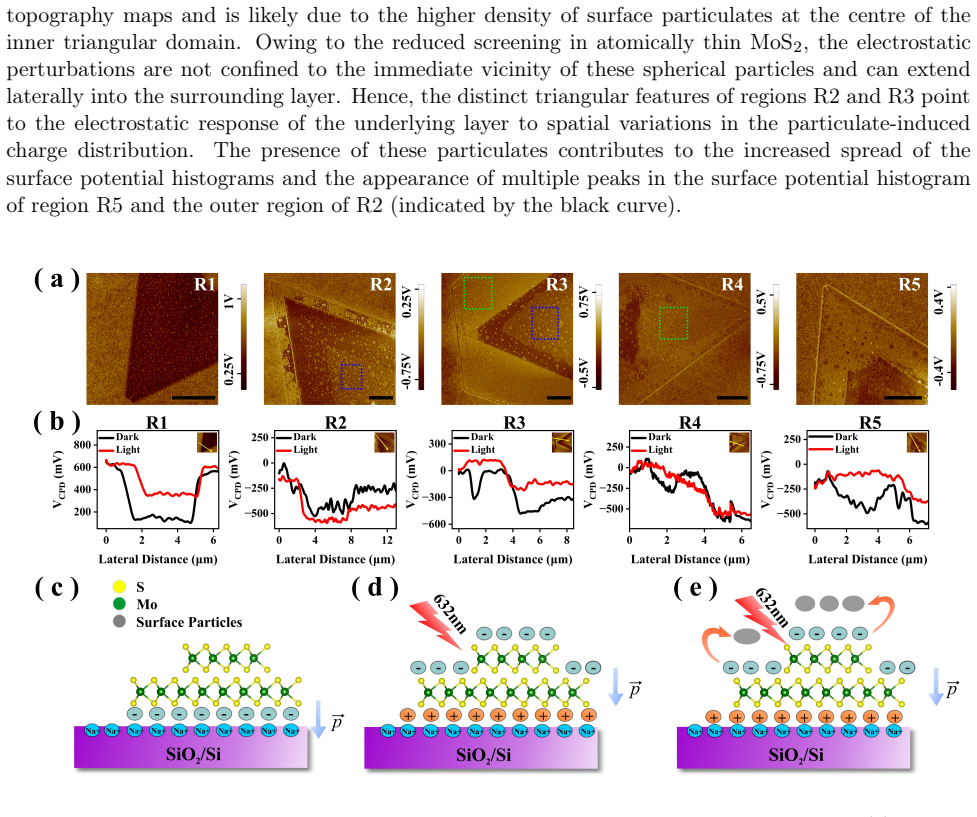
In CVD-grown MoS2, the work function increases with layer number in both AA'- and AB-stacked bilayers, yet the difference is larger in AB-stacked layers because of their stronger interlayer coupling. KPFM resolves local electronic variations caused by carrier trapping at residual surface particulates from growth. Photoinduced surface potential changes reveal n-type doping driven by photogating from trapped holes and Na+ ions at the MoS2/SiO2 interface. Correlative AFM in lateral force and force modulation modes links these electronic changes to nanomechanical response.
What carries the argument
Kelvin Probe Force Microscopy (KPFM) that extracts local work function from surface potential maps on identified AA' and AB stacked bilayer regions.
If this is right
- Optoelectronic device performance can be adjusted by choosing AB versus AA' stacking to set the work function.
- Residual particulates from CVD growth create local electronic heterogeneities that limit device uniformity.
- Substrate interface photogating contributes to n-type doping and must be accounted for in light-sensitive applications.
- Nanomechanical response correlates with electronic variations, enabling combined characterization of structure and function.
Where Pith is reading between the lines
- Minimizing particulates during growth could reduce spatial variations in work function across large-area films.
- The same stacking-dependent work function trend may appear in other TMD bilayers and could be tested on suspended samples to isolate substrate effects.
- Light could be used as an external knob to modulate local work function via the observed photogating mechanism in completed devices.
Load-bearing premise
Observed work function differences and photoresponses are caused mainly by stacking order and interlayer coupling rather than by differences in CVD growth conditions, surface particles, or substrate doping that vary between samples.
What would settle it
Identical work function values measured on AB and AA' bilayers grown under matched conditions with particulates removed, or photoresponse that changes equally on different substrates independent of stacking.
Figures
read the original abstract
Stacking order in bilayers of transition metal dichalcogenides (TMDs) controls structural symmetry and layer-to-layer interactions, offering a direct route to tune their electronic properties and enable optoelectronic applications. The work function is a key parameter that determines the electronic and optoelectronic device performance. However, a comprehensive understanding of the influence of stacking order on work function of TMDs remains limited. Herein, we employ Kelvin Probe Force Microscopy (KPFM) to probe spatial variations in surface potential and thereby determine the work function of AA'- and AB-stacked MoS2 bilayers grown using NaCl-assisted chemical vapor deposition (CVD) technique. The work function increases with layer number in both AA'- and AB-stacked MoS2, with a larger work function difference in AB-stacked layers, reflecting their stronger interlayer coupling. KPFM measurements clearly resolve local electronic heterogeneities arising from carrier trapping at residual surface particulates from CVD growth. Photoinduced surface potential variations imply n-type doping in MoS2 due to enhanced photogating from trapped holes and Na+ ions at the MoS2/SiO2 interface. Our study demonstrates the competing effects of interlayer coupling, substrate-induced photogating, and carrier trapping by surface particulates in determining the localized optoelectronic response of MoS2 bilayers. Correlative atomic force microscopy measurements in lateral force microscopy and force modulation microscopy modes probe the nanomechanical response to electronic variations. These findings provide new insights into the localized optoelectronic response of CVD-grown AA'- and AB-stacked MoS2, with significant implications for the design and reliability of optoelectronic devices.
Editorial analysis
A structured set of objections, weighed in public.
Referee Report
Summary. The manuscript uses Kelvin Probe Force Microscopy (KPFM) to map surface potential and extract work function values in AA'- and AB-stacked MoS2 bilayers grown by NaCl-assisted CVD. It reports that work function increases with layer number in both stacking configurations, with a larger difference observed for AB stacking that is attributed to stronger interlayer coupling. Photoinduced surface potential shifts are interpreted as evidence of n-type doping arising from photogating by trapped holes and Na+ ions at the MoS2/SiO2 interface, while local heterogeneities are resolved to residual CVD particulates. Correlative lateral force and force modulation AFM modes are used to link nanomechanical response to these electronic variations.
Significance. If the stacking-dependent work function trends can be shown to arise principally from interlayer coupling rather than from spatially varying Na+ incorporation or particulate trapping, the nanoscale mapping would offer useful guidance for designing TMD-based optoelectronic devices where local electronic properties matter. The explicit acknowledgment of competing substrate and growth-related effects is a strength, as is the correlative AFM data. However, the absence of reported quantitative metrics, error bars, or sample statistics in the abstract, combined with the use of NaCl-assisted growth without stated controls for precursor flux or post-annealing across stacking types, limits the immediate impact.
major comments (2)
- [Abstract and Results] Abstract and Results section: The central claim that the larger work function difference in AB-stacked layers 'reflects their stronger interlayer coupling' is load-bearing for the paper's interpretation, yet the manuscript itself notes that photoresponse is dominated by photogating from trapped holes and Na+ ions at the MoS2/SiO2 interface and that KPFM resolves heterogeneities from residual CVD particulates. No quantitative comparison (e.g., local trap density, Na+ concentration via XPS or similar, or statistics across multiple AA' vs. AB regions) is described to rule out differential ion incorporation or particulate density correlated with local stacking or growth kinetics.
- [Experimental Methods] Experimental Methods: The abstract states clear trends in work function versus layer number and stacking but provides no quantitative data, error bars, sample statistics, or detailed KPFM calibration procedures (tip work function reference, contact potential difference conversion, or humidity/illumination controls). This prevents evaluation of whether the reported AB-AA' delta exceeds measurement uncertainty or sample-to-sample variation.
minor comments (1)
- [Abstract] Abstract: The phrase 'competing effects of interlayer coupling, substrate-induced photogating, and carrier trapping' is stated but not followed by a clear statement of how these are disentangled in the data analysis or figures.
Simulated Author's Rebuttal
We thank the referee for the constructive comments and positive assessment of the work's potential significance. We have revised the manuscript to incorporate quantitative metrics, error bars, sample statistics, and expanded methodological details. Point-by-point responses to the major comments follow.
read point-by-point responses
-
Referee: [Abstract and Results] Abstract and Results section: The central claim that the larger work function difference in AB-stacked layers 'reflects their stronger interlayer coupling' is load-bearing for the paper's interpretation, yet the manuscript itself notes that photoresponse is dominated by photogating from trapped holes and Na+ ions at the MoS2/SiO2 interface and that KPFM resolves heterogeneities from residual CVD particulates. No quantitative comparison (e.g., local trap density, Na+ concentration via XPS or similar, or statistics across multiple AA' vs. AB regions) is described to rule out differential ion incorporation or particulate density correlated with local stacking or growth kinetics.
Authors: We agree that strengthening the attribution requires additional quantitative support. In the revised manuscript, we now report work-function statistics compiled from multiple AA' and AB regions across three independent samples, including standard deviations and error bars on the layer-number and stacking-dependent differences. These data show the AB–AA' delta remains larger even when restricting analysis to particulate-free areas, and the magnitude of photoinduced shifts is statistically indistinguishable between stackings. This supports interlayer coupling as the dominant origin of the stacking-dependent offset. Direct nanoscale Na+ quantification (e.g., via XPS) was not performed; we have added an explicit discussion of this limitation and note that future correlative studies could address it. revision: partial
-
Referee: [Experimental Methods] Experimental Methods: The abstract states clear trends in work function versus layer number and stacking but provides no quantitative data, error bars, sample statistics, or detailed KPFM calibration procedures (tip work function reference, contact potential difference conversion, or humidity/illumination controls). This prevents evaluation of whether the reported AB-AA' delta exceeds measurement uncertainty or sample-to-sample variation.
Authors: We have updated the abstract to include the measured work-function values with uncertainties and the number of regions/samples analyzed. The Methods section now details the KPFM calibration: tip work function referenced to freshly cleaved HOPG (4.6 eV), CPD-to-work-function conversion formula, and experimental controls for relative humidity (<30 %) and illumination conditions. These additions confirm that the reported AB–AA' differences exceed both the instrumental uncertainty (~20 mV) and observed sample-to-sample variation. revision: yes
- Direct local quantification of Na+ concentration or trap density as a function of stacking order, which would require additional experiments (e.g., spatially resolved XPS or trap-filling spectroscopy) not included in the original study.
Circularity Check
No significant circularity: purely experimental KPFM observations
full rationale
The paper consists of direct experimental measurements of surface potential via KPFM on AA'- and AB-stacked MoS2 bilayers, reporting observed increases in work function with layer number and larger differences in AB stacking. No mathematical derivations, equations, fitted parameters, or model predictions are present that could reduce to inputs by construction. Interpretations (e.g., stronger interlayer coupling) are qualitative attributions to the data rather than self-referential reductions. No self-citation chains or ansatzes are invoked as load-bearing premises. The work is self-contained empirical reporting against external benchmarks.
Axiom & Free-Parameter Ledger
axioms (2)
- domain assumption Kelvin Probe Force Microscopy accurately reports work function differences without dominant tip-sample artifacts or environmental drift
- domain assumption Stacking order (AA' vs AB) is correctly assigned from growth conditions and AFM topography
Reference graph
Works this paper leans on
-
[1]
Qing Hua Wang, Kourosh Kalantar-Zadeh, Andras Kis, Jonathan N Coleman, and Michael S Strano. Electronics and optoelectronics of two-dimensional transition metal dichalcogenides.Na- ture nanotechnology, 7(11):699–712, 2012
work page 2012
-
[2]
Single-layer mos2 transistors.Nature nanotechnology, 6(3):147–150, 2011
Branimir Radisavljevic, Aleksandra Radenovic, Jacopo Brivio, Valentina Giacometti, and Andras Kis. Single-layer mos2 transistors.Nature nanotechnology, 6(3):147–150, 2011. 12
work page 2011
-
[3]
Single-layer mos2 phototransistors.ACS nano, 6(1):74–80, 2012
Zongyou Yin, Hai Li, Hong Li, Lin Jiang, Yumeng Shi, Yinghui Sun, Gang Lu, Qing Zhang, Xiaodong Chen, and Hua Zhang. Single-layer mos2 phototransistors.ACS nano, 6(1):74–80, 2012
work page 2012
-
[4]
Wenzhuo Wu, Lei Wang, Yilei Li, Fan Zhang, Long Lin, Simiao Niu, Daniel Chenet, Xian Zhang, Yufeng Hao, Tony F Heinz, et al. Piezoelectricity of single-atomic-layer mos2 for energy conversion and piezotronics.Nature, 514(7523):470–474, 2014
work page 2014
-
[5]
Akash Singh, Manoj Dey, and Abhishek Kumar Singh. Origin of layer-dependent electrical con- ductivity of transition metal dichalcogenides.Physical Review B, 105(16):165430, 2022
work page 2022
-
[6]
Hyun-Cheol Kim, Hakseong Kim, Jae-Ung Lee, Han-Byeol Lee, Doo-Hua Choi, Jun-Ho Lee, Wi Hyoung Lee, Sung Ho Jhang, Bae Ho Park, Hyeonsik Cheong, et al. Engineering optical and electronic properties of ws2 by varying the number of layers.ACS nano, 9(7):6854–6860, 2015
work page 2015
-
[7]
Indirect-to-direct band gap crossover in few-layer mote2.Nano letters, 15(4):2336–2342, 2015
Ignacio Gutiérrez Lezama, Ashish Arora, Alberto Ubaldini, Céline Barreteau, Enrico Giannini, Marek Potemski, and Alberto F Morpurgo. Indirect-to-direct band gap crossover in few-layer mote2.Nano letters, 15(4):2336–2342, 2015
work page 2015
-
[8]
Layer dependence and light tuning surface potential of 2d mos2 on various substrates
Feng Li, Junjie Qi, Minxuan Xu, Jiankun Xiao, Yuliang Xu, Xiankun Zhang, Shuo Liu, and Yue Zhang. Layer dependence and light tuning surface potential of 2d mos2 on various substrates. Small, 13(14):1603103, 2017
work page 2017
-
[9]
Alexey Falin, Matthew Holwill, Haifeng Lv, Wei Gan, Jun Cheng, Rui Zhang, Dong Qian, Matthew R Barnett, Elton JG Santos, Konstantin S Novoselov, et al. Mechanical properties of atomically thin tungsten dichalcogenides: Ws2, wse2, and wte2.ACS nano, 15(2):2600–2610, 2021
work page 2021
-
[10]
Atomically thin mos 2: a new direct-gap semiconductor.Physical review letters, 105(13):136805, 2010
Kin Fai Mak, Changgu Lee, James Hone, Jie Shan, and Tony F Heinz. Atomically thin mos 2: a new direct-gap semiconductor.Physical review letters, 105(13):136805, 2010
work page 2010
-
[11]
Emerging photoluminescence in monolayer mos2.Nano letters, 10(4):1271–1275, 2010
Andrea Splendiani, Liang Sun, Yuanbo Zhang, Tianshu Li, Jonghwan Kim, Chi-Yung Chim, Giulia Galli, and Feng Wang. Emerging photoluminescence in monolayer mos2.Nano letters, 10(4):1271–1275, 2010
work page 2010
-
[12]
Zhiyong Y Zhu, Yingchun C Cheng, and Udo Schwingenschlögl. Giant spin-orbit-induced spin splitting in two-dimensional transition-metal dichalcogenide semiconductors.Physical Review B—Condensed Matter and Materials Physics, 84(15):153402, 2011
work page 2011
-
[13]
Valley polarization in mos2 monolayers by optical pumping.Nature nanotechnology, 7(8):490–493, 2012
Hualing Zeng, Junfeng Dai, Wang Yao, Di Xiao, and Xiaodong Cui. Valley polarization in mos2 monolayers by optical pumping.Nature nanotechnology, 7(8):490–493, 2012
work page 2012
-
[14]
Kin Fai Mak, Keliang He, Jie Shan, and Tony F Heinz. Control of valley polarization in monolayer mos2 by optical helicity.Nature nanotechnology, 7(8):494–498, 2012
work page 2012
-
[15]
Light–valley interactions in 2d semiconductors.Nature Photonics, 12(8):451–460, 2018
Kin Fai Mak, Di Xiao, and Jie Shan. Light–valley interactions in 2d semiconductors.Nature Photonics, 12(8):451–460, 2018
work page 2018
-
[16]
Strong light–matter coupling in two-dimensional atomic crystals
Xiaoze Liu, Tal Galfsky, Zheng Sun, Fengnian Xia, Erh-chen Lin, Yi-Hsien Lee, Stéphane Kéna- Cohen, and Vinod M Menon. Strong light–matter coupling in two-dimensional atomic crystals. Nature Photonics, 9(1):30–34, 2015. 13
work page 2015
-
[17]
Yuanyuan Shi, Benjamin Groven, Quentin Smets, Surajit Sutar, Sreetama Banerjee, Henry Med- ina, Xiangyu Wu, Cedric Huyghebaert, Steven Brems, Dennis Lin, et al. Superior electrostatic control in uniform monolayer mos 2 scaled transistors via in-situ surface smoothening. In2021 IEEE International Electron Devices Meeting (IEDM), pages 37–1. IEEE, 2021
work page 2021
-
[18]
Sudipta Majumder, Sarika Lohkna, Vaibhav Walve, Rahul Chand, Gokul M Anilkumar, Sooyeon Hwang, GV Pavan Kumar, Aparna Deshpande, Prasenjit Ghosh, and Atikur Rahman. Unveiling the correlation between defects and high mobility in mos2 monolayers.ACS Applied Materials & Interfaces, 17(7):10942–10953, 2025
work page 2025
-
[19]
Sensing behavior of atomically thin-layered mos2 transistors.ACS nano, 7(6):4879–4891, 2013
Dattatray J Late, Yi-Kai Huang, Bin Liu, Jagaran Acharya, Sharmila N Shirodkar, Jiajun Luo, Aiming Yan, Daniel Charles, Umesh V Waghmare, Vinayak P Dravid, et al. Sensing behavior of atomically thin-layered mos2 transistors.ACS nano, 7(6):4879–4891, 2013
work page 2013
-
[20]
Xiumei Zhang, Haiyan Nan, Shaoqing Xiao, Xi Wan, Xiaofeng Gu, Aijun Du, Zhenhua Ni, and Kostya Ostrikov. Transition metal dichalcogenides bilayer single crystals by reverse-flow chemical vapor epitaxy.Nature communications, 10(1):598, 2019
work page 2019
-
[21]
Hai Li, Zongyou Yin, Qiyuan He, Hong Li, Xiao Huang, Gang Lu, Derrick Wen Hui Fam, Alfred Iing Yoong Tok, Qing Zhang, and Hua Zhang. Fabrication of single-and multilayer mos2 film-based field-effect transistors for sensing no at room temperature.small, 8(1):63–67, 2012
work page 2012
-
[22]
Zai-Quan Xu, Yupeng Zhang, Ziyu Wang, Yuting Shen, Wenchao Huang, Xue Xia, Wenzhi Yu, Yunzhou Xue, Litao Sun, Changxi Zheng, et al. Atomically thin lateral p–n junction photodetector with large effective detection area.2D Materials, 3(4):041001, 2016
work page 2016
-
[23]
Wenzhong Bao, Xinghan Cai, Dohun Kim, Karthik Sridhara, and Michael S Fuhrer. High mobility ambipolar mos2 field-effect transistors: Substrate and dielectric effects.Applied Physics Letters, 102(4):042104, 2013
work page 2013
-
[24]
Carter Fox, Yulu Mao, Xiang Zhang, Ying Wang, and Jun Xiao. Stacking order engineering of two-dimensional materials and device applications.Chemical Reviews, 124(4):1862–1898, 2023
work page 2023
-
[25]
Trond I Andersen, Giovanni Scuri, Andrey Sushko, Kristiaan De Greve, Jiho Sung, You Zhou, Dominik S Wild, Ryan J Gelly, Hoseok Heo, Damien Bérubé, et al. Excitons in a reconstructed moiré potential in twisted wse2/wse2 homobilayers.Nature materials, 20(4):480–487, 2021
work page 2021
-
[26]
Superconductivity in twisted bilayer wse2.Nature, 637(8047):833–838, 2025
Yiyu Xia, Zhongdong Han, Kenji Watanabe, Takashi Taniguchi, Jie Shan, and Kin Fai Mak. Superconductivity in twisted bilayer wse2.Nature, 637(8047):833–838, 2025
work page 2025
-
[27]
Moiré phonons in twisted bilayer mos2.Acs Nano, 12(8):8770–8780, 2018
Miao-Ling Lin, Qing-Hai Tan, Jiang-Bin Wu, Xiao-Shuang Chen, Jin-Huan Wang, Yu-Hao Pan, Xin Zhang, Xin Cong, Jun Zhang, Wei Ji, et al. Moiré phonons in twisted bilayer mos2.Acs Nano, 12(8):8770–8780, 2018
work page 2018
-
[28]
Astrid Weston, Eli G Castanon, Vladimir Enaldiev, Fabio Ferreira, Shubhadeep Bhattacharjee, Shuigang Xu, Héctor Corte-León, Zefei Wu, Nicholas Clark, Alex Summerfield, et al. Interfacial ferroelectricity in marginally twisted 2d semiconductors.Nature nanotechnology, 17(4):390–395, 2022
work page 2022
-
[29]
Lei Wang, En-Min Shih, Augusto Ghiotto, Lede Xian, Daniel A Rhodes, Cheng Tan, Martin Claassen, Dante M Kennes, Yusong Bai, Bumho Kim, et al. Correlated electronic phases in twisted bilayer transition metal dichalcogenides.Nature materials, 19(8):861–866, 2020. 14
work page 2020
-
[30]
Twist-dependent tuning of excitonic emis- sions in bilayer wse2.ACS omega, 7(7):6412–6418, 2022
Prahalad Kanti Barman, Pranshoo Upadhyay, Ramesh Rajarapu, Sharad Kumar Yadav, Latha KVP, Meenakshisundaram N, and Pramoda K Nayak. Twist-dependent tuning of excitonic emis- sions in bilayer wse2.ACS omega, 7(7):6412–6418, 2022
work page 2022
-
[31]
Arend M Van Der Zande, Jens Kunstmann, Alexey Chernikov, Daniel A Chenet, YuMeng You, XiaoXiao Zhang, Pinshane Y Huang, Timothy C Berkelbach, Lei Wang, Fan Zhang, et al. Tai- loring the electronic structure in bilayer molybdenum disulfide via interlayer twist.Nano letters, 14(7):3869–3875, 2014
work page 2014
-
[32]
Bumho Kim, Jicheng Jin, Zhi Wang, Li He, Thomas Christensen, Eugene J Mele, and Bo Zhen. Three-dimensional nonlinear optical materials from twisted two-dimensional van der waals inter- faces.Nature Photonics, 18(1):91–98, 2024
work page 2024
-
[33]
Jiaxu Yan, Juan Xia, Xingli Wang, Lei Liu, Jer-Lai Kuo, Beng Kang Tay, Shoushun Chen, Wu Zhou, Zheng Liu, and Ze Xiang Shen. Stacking-dependent interlayer coupling in trilayer mos2 with broken inversion symmetry.Nano letters, 15(12):8155–8161, 2015
work page 2015
-
[34]
Jiangang He, Kerstin Hummer, and Cesare Franchini. Stacking effects on the electronic and optical properties of bilayer transition metal dichalcogenides mos 2, mose 2, ws 2, and wse 2.Physical Review B, 89(7):075409, 2014
work page 2014
-
[35]
Ming Xia, Bo Li, Kuibo Yin, Giovanni Capellini, Gang Niu, Yongji Gong, Wu Zhou, Pulickel M Ajayan, and Ya-Hong Xie. Spectroscopic signatures of aa’ and ab stacking of chemical vapor deposited bilayer mos2.ACS nano, 9(12):12246–12254, 2015
work page 2015
-
[36]
Zhequan Yan, Liang Chen, Mina Yoon, and Satish Kumar. The role of interfacial electronic prop- erties on phonon transport in two-dimensional mos2 on metal substrates.ACS applied materials & interfaces, 8(48):33299–33306, 2016
work page 2016
-
[37]
Ioannis Paradisanos, Shivangi Shree, Antony George, Nadine Leisgang, Cedric Robert, Kenji Watanabe, Takashi Taniguchi, Richard J Warburton, Andrey Turchanin, Xavier Marie, et al. Controlling interlayer excitons in mos2 layers grown by chemical vapor deposition.Nature com- munications, 11(1):2391, 2020
work page 2020
-
[38]
Hanjun Jiang, Lei Li, Yao Wu, Ruihuan Duan, Kongyang Yi, Lishu Wu, Chao Zhu, Lei Luo, Manzhang Xu, Lu Zheng, et al. Vapor deposition of bilayer 3r mos2 with room-temperature ferroelectricity.Advanced Materials, 36(32):2400670, 2024
work page 2024
-
[39]
Strain-engineered ferroelectricity in 2h bilayer mos2.ACS nano, 18(44):30360–30367, 2024
Jianfeng Mao, Jingyu He, Weng Fu Io, Feng Guo, Zehan Wu, Ming Yang, and Jianhua Hao. Strain-engineered ferroelectricity in 2h bilayer mos2.ACS nano, 18(44):30360–30367, 2024
work page 2024
-
[40]
Vishnu Aggarwal, Irfan H Abidi, Jake Limb, Clara Kofler, Ajay Kumar Verma, Sindhu Priya Giridhar, Nethmi SL Dissanayake, Pargam Vashishtha, Jonathan O Tollerud, Jianfeng Mao, et al. Stacking mode-driven enhancement of optoelectronic and electrocatalytic properties in bilayer 2h mos2.ACS Applied Materials & Interfaces, 17(34):48658–48669, 2025
work page 2025
-
[41]
Manzhang Xu, Hongjia Ji, Lu Zheng, Weiwei Li, Jing Wang, Hanxin Wang, Lei Luo, Qianbo Lu, Xuetao Gan, Zheng Liu, et al. Reconfiguring nucleation for cvd growth of twisted bilayer mos2 with a wide range of twist angles.Nature Communications, 15(1):562, 2024
work page 2024
-
[42]
Seong Chul Hong, Ji-Hwan Baek, Jinwoo Kim, Hyeongseok Lee, and Gwan-Hyoung Lee. Strain- mediatedcontrolofdomainstructuresin3r-mos2bilayerssynthesizedbyvapor–liquid–solidgrowth in chemical vapor deposition.ACS nano, 19(33):30487–30494, 2025. 15
work page 2025
-
[43]
Denghui Yan, Binbin Ding, Lihan Wang, Lianbi Li, Xiaolong Ren, Jiangbin Li, Qinglong Fang, Dezhong Cao, Guoqing Zhang, Caijuan Xia, et al. Preparation and properties of bilayer mos2 with different stacking structures.Applied Surface Science, 695:162875, 2025
work page 2025
-
[44]
Aditya Singh, Monika Moun, Madan Sharma, Arabinda Barman, Ashok Kumar Kapoor, and Rajendra Singh. Nacl-assisted substrate dependent 2d planar nucleated growth of mos2.Applied Surface Science, 538:148201, 2021
work page 2021
-
[45]
Lili Zhang, Chenyu Wang, Xue-Lu Liu, Tao Xu, Mingsheng Long, Erfu Liu, Chen Pan, Guangxu Su, Junwen Zeng, Yajun Fu, et al. Damage-free and rapid transfer of cvd-grown two-dimensional transition metal dichalcogenides by dissolving sacrificial water-soluble layers. Nanoscale, 9(48):19124–19130, 2017
work page 2017
-
[46]
Dingding Jiang, Xuejun Wang, Renzhong Chen, Jiang Sun, Hua Kang, Daizong Ji, Yunqi Liu, and Dacheng Wei. Self-expanding molten salt-driven growth of patterned transition-metal dichalco- genide crystals.Journal of the American Chemical Society, 144(19):8746–8755, 2022
work page 2022
-
[47]
Kehao Zhang, Brian M Bersch, Fu Zhang, Natalie C Briggs, Shruti Subramanian, Ke Xu, Mikhail Chubarov, Ke Wang, Jordan O Lerach, Joan M Redwing, et al. Considerations for utilizing sodium chloride in epitaxial molybdenum disulfide.ACS applied materials & interfaces, 10(47):40831– 40837, 2018
work page 2018
-
[48]
Xiai Luo, Zhenghan Peng, Zegao Wang, and Mingdong Dong. Layer-by-layer growth of aa-stacking mos2 for tunable broadband phototransistors.ACS Applied Materials & Interfaces, 13(49):59154– 59163, 2021
work page 2021
-
[49]
Shuang Wang, Yanhui Zhang, Dongyang Zhao, Jing Li, He Kang, Sunwen Zhao, Tingting Jin, Jiaxiang Zhang, Zhongying Xue, Ying Wang, et al. Fast and controllable synthesis of ab-stacked bilayer mos2 for photoelectric detection.2D Materials, 9(1):015016, 2022
work page 2022
-
[50]
Aiqing Fan, Qing Zhang, Zebin Ren, Lin Li, Ziyi Han, Weijie Ma, Xianfeng Shen, Jichen Dong, Xi Yu, Dechao Geng, et al. Layer number and stacking engineering of mos2 crystals for high-performance polarization-sensitive photodetector.ACS Applied Materials & Interfaces, 16(43):59626–59636, 2024
work page 2024
-
[51]
Shangzhi Gu, Wenyu Liu, Shuo Mi, Guoyu Xian, Jiangfeng Guo, Fei Pang, Shanshan Chen, Haitao Yang, Hong-Jun Gao, and Zhihai Cheng. Twist angle-dependent work functions in cvd-grown twisted bilayer graphene probed by kelvin probe force microscopy.Nanoscale, 15(12):5825–5833, 2023
work page 2023
-
[52]
Francesco Lavini, Annalisa Calò, Yang Gao, Edoardo Albisetti, Tai-De Li, Tengfei Cao, Guoqing Li, Linyou Cao, Carmela Aruta, and Elisa Riedo. Friction and work function oscillatory behavior for an even and odd number of layers in polycrystalline mos 2.Nanoscale, 10(17):8304–8312, 2018
work page 2018
-
[53]
Vishakha Kaushik, Deepak Varandani, and BR Mehta. Nanoscale mapping of layer-dependent surface potential and junction properties of cvd-grown mos2 domains.The Journal of Physical Chemistry C, 119(34):20136–20142, 2015
work page 2015
-
[54]
SooHo Choi, Zhang Shaolin, and Woochul Yang. Layer-number-dependent work function of mos2 nanoflakes.Journal of the Korean Physical Society, 64(10):1550–1555, 2014. 16
work page 2014
-
[55]
Jong Hun Kim, Jinhwan Lee, Jae Hyeon Kim, CC Hwang, Changgu Lee, and Jeong Young Park. Workfunctionvariationofmos2atomiclayersgrownwithchemicalvapordeposition: Theeffectsof thickness and the adsorption of water/oxygen molecules.Applied Physics Letters, 106(25):251606, 2015
work page 2015
-
[56]
Woongbin Yim, Van Tu Nguyen, Quynh Thi Phung, Hwan Sik Kim, Yeong Hwan Ahn, Soonil Lee, and Ji-Yong Park. Imaging spatial distribution of photogenerated carriers in monolayer mos2 with kelvin probe force microscopy.ACS Applied Materials & Interfaces, 14(22):26295–26302, 2022
work page 2022
-
[57]
Xiaoxu Zhao, Weitao Su, Fei Chen, and Hongwei Lu. Localized optoelectronic responses in the reconstructed moiré superlattice of twisted bilayer mos2.ACS Applied Electronic Materi- als, 7(2):687–695, 2025
work page 2025
-
[58]
Astrid Weston, Yichao Zou, Vladimir Enaldiev, Alex Summerfield, Nicholas Clark, Viktor Zóly- omi, Abigail Graham, Celal Yelgel, Samuel Magorrian, Mingwei Zhou, et al. Atomic reconstruc- tion in twisted bilayers of transition metal dichalcogenides.Nature nanotechnology, 15(7):592–597, 2020
work page 2020
-
[59]
G Anagha, Kalyan Ghosh, Pratap Kumar Sahoo, and Jyoti Mohanty. Unveiling thermally driven photoluminescence in cvd grown mos2 dendritic flake.Physica E: Low-dimensional Systems and Nanostructures, 165:116065, 2025
work page 2025
-
[60]
Anagha Gopinath, Faiha Mujeeb, Subhabrata Dhar, and Jyoti Mohanty. Optically active de- fect states and valley depolarization in monolayer mos 2 induced by high-energy electron-beam irradiation.Nanoscale, 2026
work page 2026
-
[61]
Sachin M Shinde, Krishna P Dhakal, Xiang Chen, Won Seok Yun, JaeDong Lee, Hyunmin Kim, and Jong-Hyun Ahn. Stacking-controllable interlayer coupling and symmetric configuration of multilayered mos2.NPG Asia Materials, 10(2):e468–e468, 2018
work page 2018
-
[62]
Stacking-dependent optical properties in bilayer wse 2.Nanoscale, 14(1):147–156, 2022
KathleenMMcCreary, MadeleinePhillips, Hsun-JenChuang, DarshanaWickramaratne, Matthew Rosenberger, C Stephen Hellberg, and Berend T Jonker. Stacking-dependent optical properties in bilayer wse 2.Nanoscale, 14(1):147–156, 2022
work page 2022
-
[63]
Haoyu Dong, Songyang Li, Shuo Mi, Jianfeng Guo, Zhaxi Suonan, Hanxiang Wu, Yanyan Geng, Manyu Wang, Huiwen Xu, Li Guan, et al. Strain-engineered rippling at the bilayer-mos2 interface identified by advanced atomic force microscopy.Frontiers of Physics, 19(6):63201, 2024
work page 2024
-
[64]
Vapour–liquid–solid growth of monolayer mos2 nanoribbons.Nature materials, 17(6):535–542, 2018
Shisheng Li, Yung-Chang Lin, Wen Zhao, Jing Wu, Zhuo Wang, Zehua Hu, Youde Shen, Dai- Ming Tang, Junyong Wang, Qi Zhang, et al. Vapour–liquid–solid growth of monolayer mos2 nanoribbons.Nature materials, 17(6):535–542, 2018
work page 2018
-
[65]
Jinfeng Yang, Ye Fan, Ryo Mizuta, Max Rimmer, Jack Donoghue, Shaoliang Guan, Sarah J Haigh, and Stephan Hofmann. Operando scanning electron microscopy study of support interactions and mechanisms of salt-assisted ws2 growth.Chemistry of Materials, 37(3):989–1000, 2025
work page 2025
-
[66]
Mahima Tyagi, Srijata Dey, Pinky Sahoo, and Deshdeep Sahdev. Systematic study of cvd-growth parameters in nacl-assisted growth of mose 2 nanostructures: nanoribbons, dendrites and spirals. Materials Advances, 2025. 17
work page 2025
-
[67]
Pallavi Aggarwal, Shuchi Kaushik, Prashant Bisht, Madan Sharma, Aditya Singh, Bodh Raj Mehta, and Rajendra Singh. Centimeter-scale synthesis of monolayer ws2 using single-zone atmospheric-pressure chemical vapor deposition: a detailed study of parametric dependence, growth mechanism, and photodetector properties.Crystal Growth & Design, 22(5):3206–3217, 2022
work page 2022
-
[68]
Syed Hamza Safeer, Alexandre SM Ore, Alisson R Cadore, Vanessa O Gordo, Pilar G Vianna, Isabel Carvalho, Victor Carozo, and Christiano JS de Matos. Cvd growth and optical characteri- zation of homo and heterobilayer tmds.Journal of Applied Physics, 132(2):024301, 2022
work page 2022
-
[69]
From bulk to monolayer mos2: evolution of raman scattering
Hong Li, Qing Zhang, Chin Chong Ray Yap, Beng Kang Tay, Teo Hang Tong Edwin, Aurelien Olivier, and Dominique Baillargeat. From bulk to monolayer mos2: evolution of raman scattering. Advanced Functional Materials, 22(7):1385–1390, 2012
work page 2012
-
[70]
Muhammad Suleman, Sohee Lee, Minwook Kim, Van Huy Nguyen, Muhammad Riaz, Naila Nasir, Sunil Kumar, Hyun Min Park, Jongwan Jung, and Yongho Seo. Nacl-assisted temperature- dependent controllable growth of large-area mos2 crystals using confined-space cvd.ACS omega, 7(34):30074–30086, 2022
work page 2022
-
[71]
In Soo Kim, Vinod K Sangwan, Deep Jariwala, Joshua D Wood, Spencer Park, Kan-Sheng Chen, Fengyuan Shi, Francisco Ruiz-Zepeda, Arturo Ponce, Miguel Jose-Yacaman, et al. Influence of stoichiometry on the optical and electrical properties of chemical vapor deposition derived mos2. ACS nano, 8(10):10551–10558, 2014
work page 2014
-
[72]
Long Chen, Lingyu Zang, Luhua Chen, Jinchao Wu, Chengming Jiang, and Jinhui Song. Study on the catalyst effect of nacl on mos 2 growth in a chemical vapor deposition process.CrystEngComm, 23(31):5337–5344, 2021
work page 2021
-
[73]
Sang Wook Han, Won Seok Yun, Whang Je Woo, Hyungjun Kim, Jusang Park, Young Hun Hwang, Tri Khoa Nguyen, Chinh Tam Le, Yong Soo Kim, Manil Kang, et al. Interface defect engineering of a large-scale cvd-grown mos2 monolayer via residual sodium at the sio2/si substrate. Advanced Materials Interfaces, 8(14):2100428, 2021
work page 2021
-
[74]
Vishakha Kaushik, Mujeeb Ahmad, Khushboo Agarwal, Deepak Varandani, Branson D Belle, Pintu Das, and BR Mehta. Charge transport in 2d mos2, ws2, and mos2–ws2 heterojunction-based field-effect transistors: Role of ambipolarity.The Journal of Physical Chemistry C, 124(42):23368– 23379, 2020
work page 2020
-
[75]
Stacking-dependent interlayer phonons in 3r and 2h mos2.2D Materials, 6(2):025022, 2019
Jeremiah Van Baren, Gaihua Ye, Jia-An Yan, Zhipeng Ye, Pouyan Rezaie, Peng Yu, Zheng Liu, Rui He, and Chun Hung Lui. Stacking-dependent interlayer phonons in 3r and 2h mos2.2D Materials, 6(2):025022, 2019
work page 2019
-
[76]
Modulation of electronic properties from stacking orders and spin-orbit coupling for 3r-type mos2
Xiaofeng Fan, WT Zheng, Jer-Lai Kuo, David J Singh, Chang Qing Sun, and Weiguang Zhu. Modulation of electronic properties from stacking orders and spin-orbit coupling for 3r-type mos2. Scientific reports, 6(1):24140, 2016
work page 2016
-
[77]
Joachim Jelken, María O Avilés, and François Lagugné-Labarthet. The hidden flower in ws2 flakes: a combined nanomechanical and tip-enhanced raman exploration.ACS nano, 16(8):12352–12363, 2022. 18
work page 2022
discussion (0)
Sign in with ORCID, Apple, or X to comment. Anyone can read and Pith papers without signing in.